Surface wave launcher
- Summary
- Abstract
- Description
- Claims
- Application Information
AI Technical Summary
Benefits of technology
Problems solved by technology
Method used
Image
Examples
Embodiment Construction
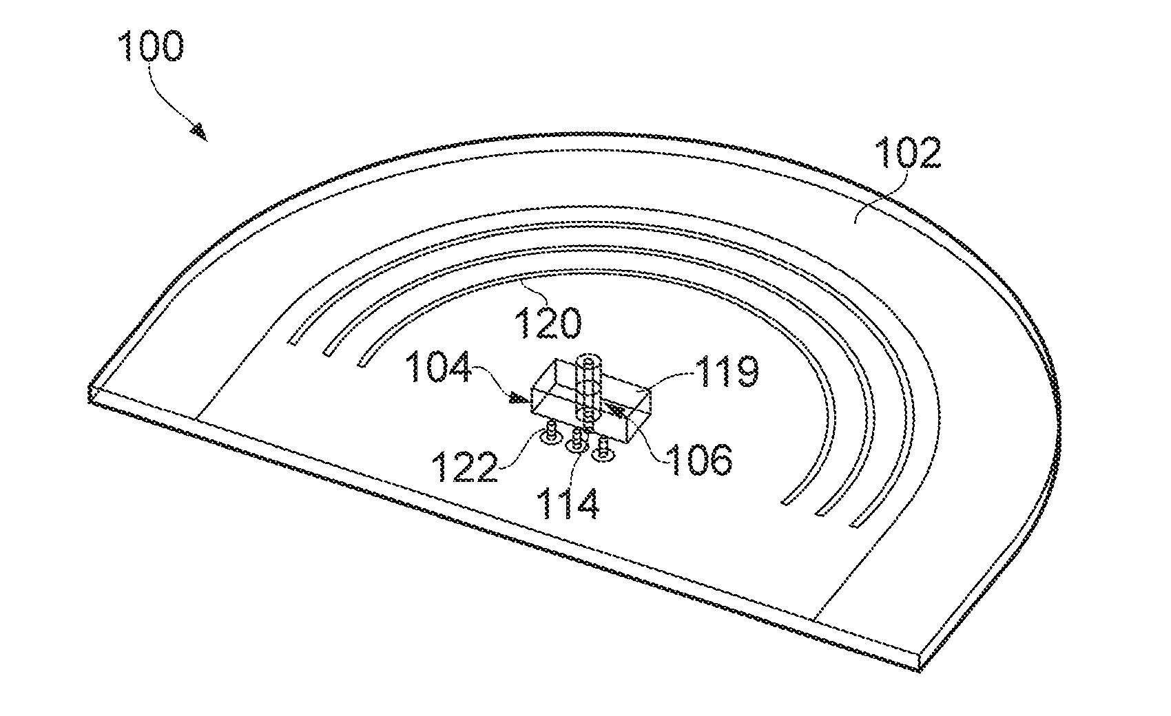
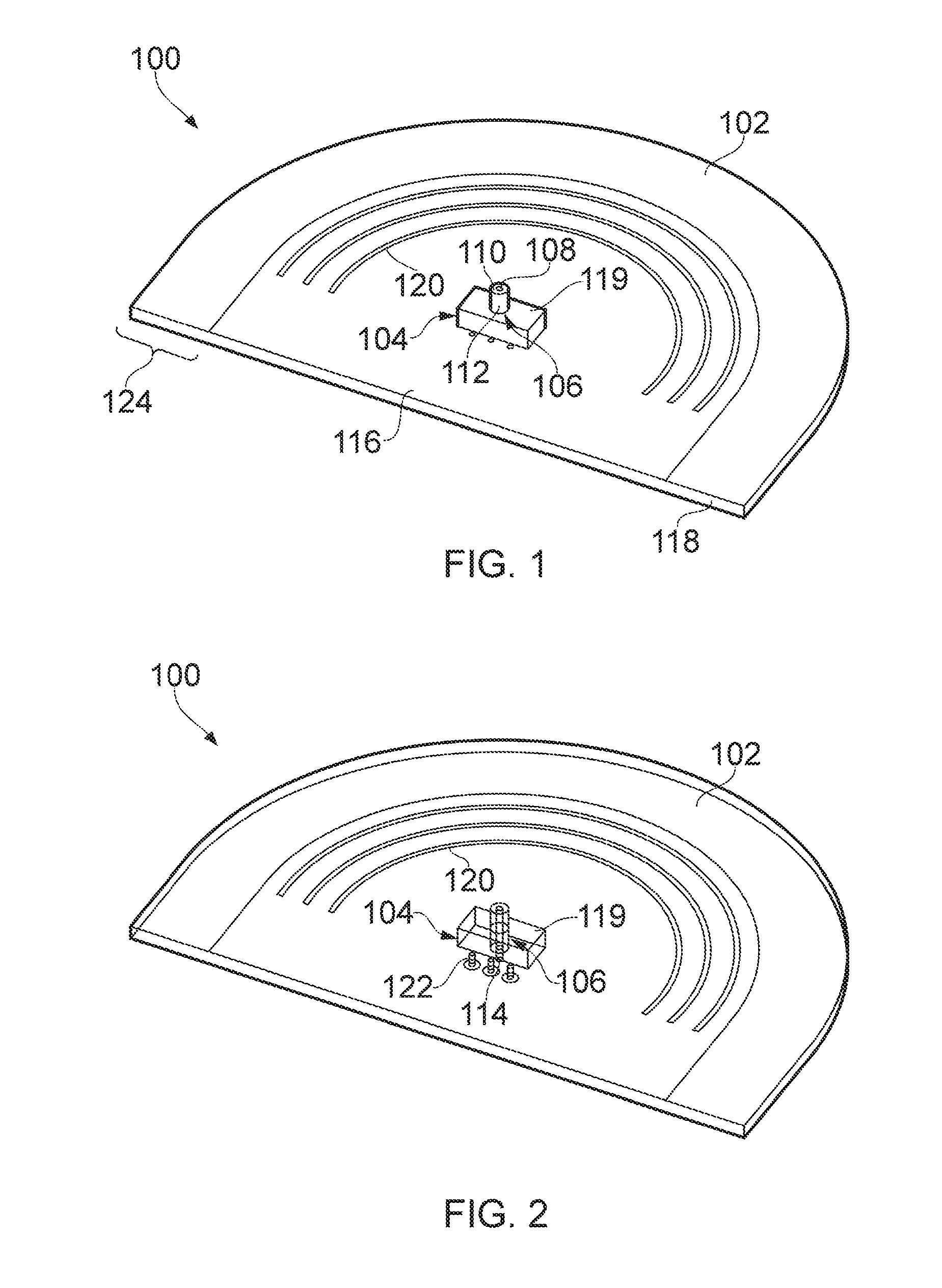
[0013]FIGS. 1 and 2 show a surface wave launcher 100 in accordance with an embodiment of the present invention. The surface wave launcher 100 includes a waveguide section 102 and a feed section 104. The feed section 104 comprises a coaxial cable 106. The coaxial cable 106 includes an inner conductor 108, an insulating layer 110 and an outer conductor 112. The feed section 104 also includes a feed pin 114 which is connected to the inner conductor 108 at the end of the coaxial cable 106 and couples the inner conductor 108 to the waveguide 102.
[0014]The waveguide 102 comprises a planar conductor 116, which forms an upper surface of the waveguide 102. The waveguide 102 preferably also comprises a dielectric layer 118, positioned below the planar conductor 116. The dielectric making up the dielectric layer 118 is preferably low loss for the wavelength of operation, i.e. the wavelength of surface waves to be launched. The launcher 100 can use substrates having a low dielectric constant. I...
PUM
 Abstract
Description
Claims
Application Information


