Eureka AIR delivers breakthrough ideas for toughest innovation challenges, trusted by R&D personnel around the world.

Method for forming patterned structure

a patterned structure and pattern technology, applied in the field of forming a pattern structure, can solve the problems of affecting the performance of the semiconductor device, and the design of the integrated circuit will be limited accordingly, so as to achieve the effect of improving the similarity between the layout pattern and the pattern structur

Active Publication Date: 2019-10-01
UNITED MICROELECTRONICS CORP
View PDF6 Cites 0 Cited by
  • Summary
  • Abstract
  • Description
  • Claims
  • Application Information

AI Technical Summary

Benefits of technology

[0004]It is one of the objectives of the present invention to provide a method for forming a patterned structure. Lines elongated in different directions in a layout pattern are decomposed into two masks. Two photolithography processes with these two masks respectively are performed for forming a patterned structure including line structures elongated in different directions. The similarity between the layout pattern and the patterned structure may be improved accordingly.

Problems solved by technology

However, in the photolithographic process, deviations often occur when the patterns on the photomask are transferred onto the wafer surface and jeopardize the performance of the semiconductor device.
The manufactured patterns may not be exactly identical to the layout design, and the integrated circuit design will be limited accordingly.

Method used


Image

  • Method for forming patterned structure
  • Method for forming patterned structure
  • Method for forming patterned structure

Examples


Embodiment Construction

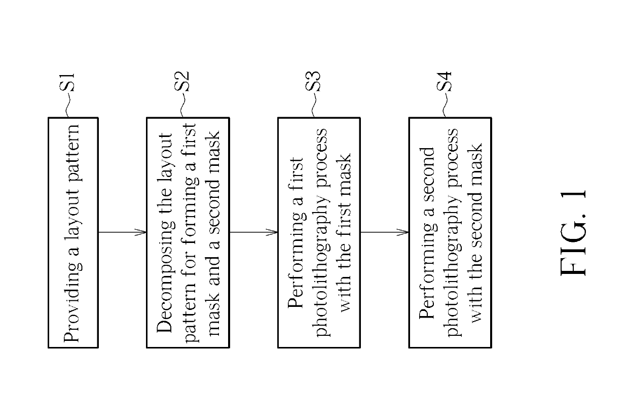
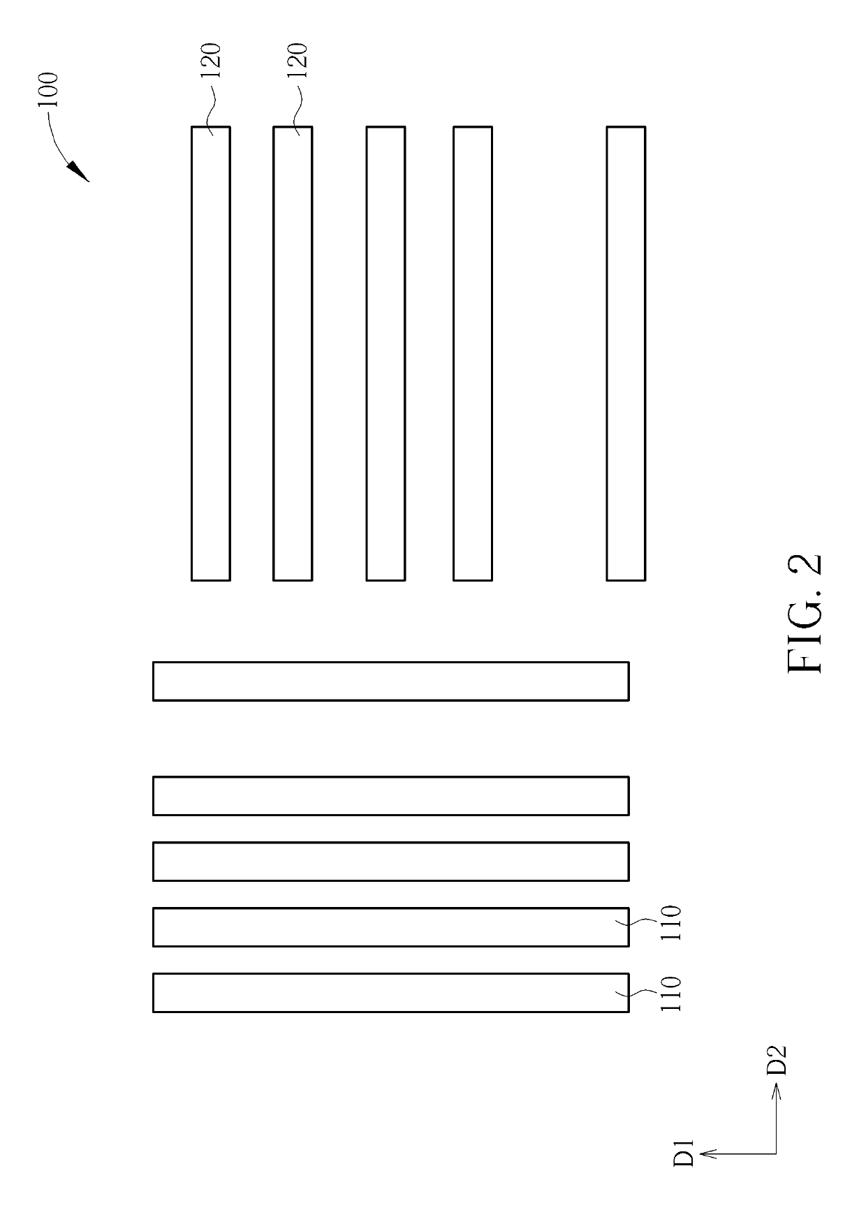
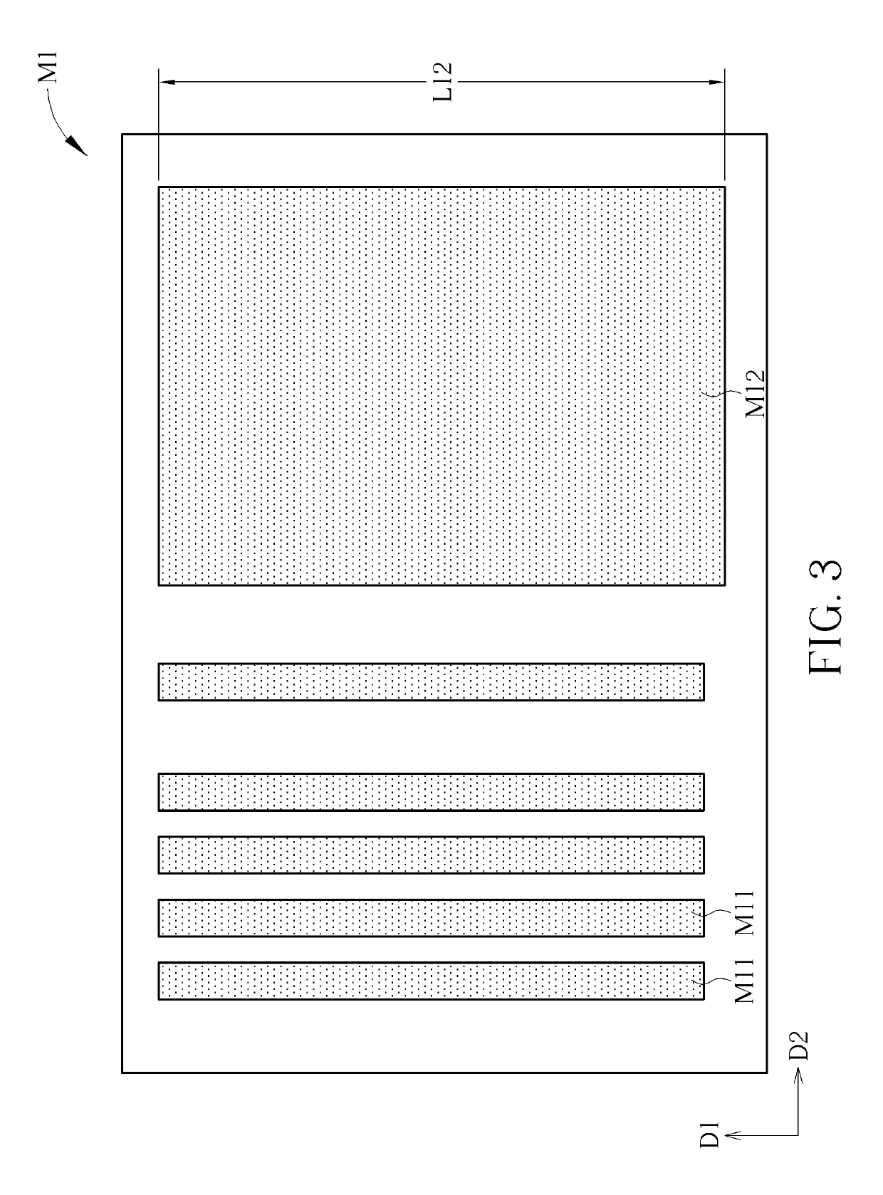
[0023]Please refer to FIGS. 1-12FIG. 1 is a flow chart of a method for forming a patterned structure according to a first embodiment of the present invention. FIG. 2 is a schematic drawing illustrating a layout pattern in this embodiment. FIG. 3 is a schematic drawing illustrating a first mask in this embodiment. FIG. 4 is a schematic drawing illustrating a second mask in this embodiment. FIG. 5 is a schematic drawing illustrating an overlapping relation between the first mask and the second mask in this embodiment. FIGS. 6-12 are schematic drawings illustrating the method for forming the patterned structure in this embodiment. The method for forming the patterned structure in this embodiment includes the following steps. As shown in FIGS. 1-5, in step S1, a layout pattern 100 is provided. The layout pattern 100 includes a plurality of first lines 110 and a plurality of second lines 120. Each of the first lines 110 is elongated in a first direction D1, and each of the second lines 1...


PUM

PropertyMeasurementUnit
structureaaaaaaaaaa
areaaaaaaaaaaa
length L12aaaaaaaaaa

Abstract

A method for forming a patterned structure includes following steps. First lines elongated in a first direction and second lines elongated in a second direction in a layout pattern are decomposed into two masks. A first mask includes first line patterns and a first block pattern. A second mask includes second line patterns and a second block pattern. Two photolithography processes with the first mask and the second mask are performed for forming a patterned structure including first line structures and second line structures. Each first line structure is elongated in the first direction. The first line structures are defined by a region where the first line patterns and the second block pattern overlap with one another. Each second line structure is elongated in the second direction. The second line structures are defined by a region where the second line patterns and the first block pattern overlap with one another.

Description

BACKGROUND OF THE INVENTION1. Field of the Invention[0001]The present invention relates to a method for forming a patterned structure, and more particularly, to a method for forming a patterned structure including line structures elongated in different directions.2. Description of the Prior Art[0002]In semiconductor manufacturing processes, in order to transfer an integrated circuit onto a semiconductor wafer, the integrated circuits from a database are first designed as a layout pattern and a photomask is then manufactured according to the layout pattern. Patterns on the photomask may then be able to be transferred to the semiconductor wafer. The steps mentioned above may be regarded as a photolithographic process. The layout pattern has to be extremely accurate for forming delicate integrated circuits so as to align with the patterns of the previous and following steps.[0003]However, in the photolithographic process, deviations often occur when the patterns on the photomask are tr...

Claims


Application Information

Patent Timeline
Patent Type & Authority Patents(United States)
IPC IPC(8): G03F1/70G03F7/20G03F7/00H01L21/027
CPCG03F7/0035G03F7/203H01L21/0274
Inventor LIOU, EN-CHIUANTUNG, YU-CHENG
Owner UNITED MICROELECTRONICS CORP
Why Eureka
Eureka Blog
Learn More