
Pixel structure of liquid crystal display panel and display device using same

a liquid crystal display panel and display device technology, applied in static indicating devices, instruments, non-linear optics, etc., can solve problems such as color shift problems, and achieve the effect of effectively resolving and alleviating whiting problems

Active Publication Date: 2019-10-15
HKC CORP LTD +1
View PDF12 Cites 0 Cited by
  • Summary
  • Abstract
  • Description
  • Claims
  • Application Information

AI Technical Summary

Benefits of technology

[0006]To resolve the foregoing technical problem, an objective of this application is to provide a design method for alleviating color shift problems, and in particular, relates to a pixel structure of a liquid crystal display panel and a display device using same, so as to effectively resolve color shift problems and effectively improve a pixel design aperture ratio.
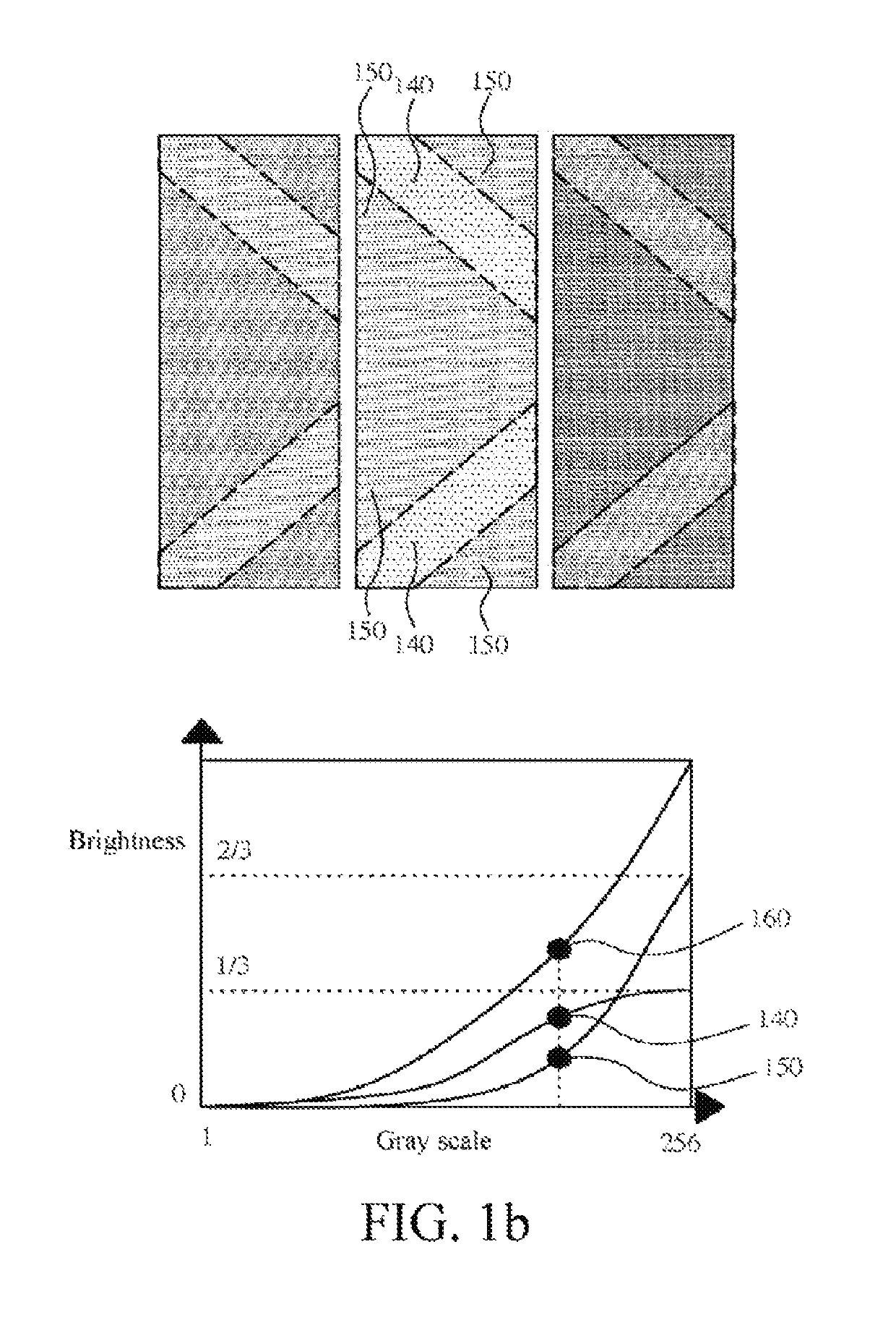
[0018]Beneficial effects of this application are effectively resolving color shift problems of the liquid crystal display panel and alleviating a whiting problem at a large visual angle.

Problems solved by technology

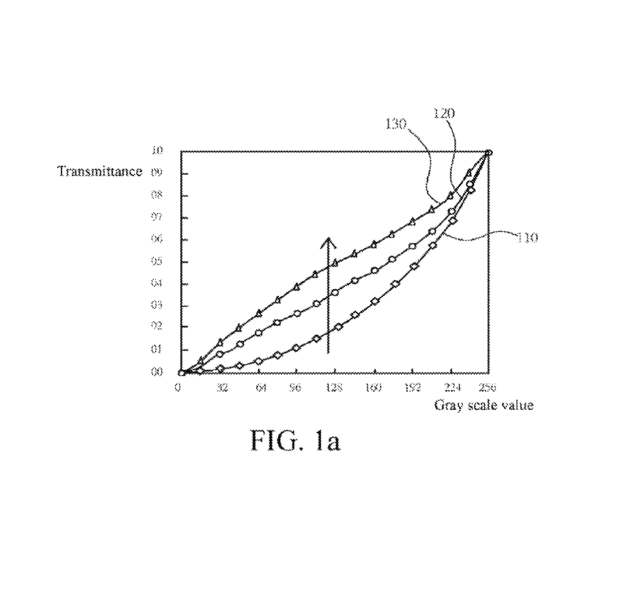
In addition, transmittances of the red light, the green light, and the blue light in film surfaces, such as a polyimide (PI) film, a planarization layer (PFA), and a coating layer (OC), in a panel are different, and consequently, a color shift problem occurs.

Method used


Image

  • Pixel structure of liquid crystal display panel and display device using same
  • Pixel structure of liquid crystal display panel and display device using same
  • Pixel structure of liquid crystal display panel and display device using same

Examples


Embodiment Construction

[0029]The following embodiments are described with reference to accompany drawings, and are used to exemplarily show particular embodiments that can be implemented and that is in this application. Direction terms mentioned in this application, such as “upper”, “lower”, “front”, “rear”, “left”, “right”, “inner”, “outer”, and “side” are only directions with reference to the accompanying drawings. Therefore, the used direction terms are used to describe and explain this application, and are not used to limit this application.

[0030]The accompany drawings and description are considered to be substantially exemplary, and are not intended for limitation. In the drawings, units with similar structures are represented by same numerals. In addition, to facilitate understanding and description, a size and a thickness of each component shown in the accompany drawings are arbitrarily shown, and this application is not limited thereto.

[0031]In the accompany drawings, for a clearance purpose, a th...


PUM

PropertyMeasurementUnit
area ratioaaaaaaaaaa
phaseaaaaaaaaaa
pixel structureaaaaaaaaaa

Abstract

This application relates to a pixel structure of a liquid crystal display panel and a display device using same, including: a plurality of pixel units, each of the pixel units includes a first light penetration area, a second light penetration area, and a third light penetration area, and a transmitting effects of the pixel units are distinguished according to different retardations and an area ratio.

Description

BACKGROUNDTechnical Field[0001]This application relates to a design method for alleviating color shift problems of a liquid crystal display panel, and in particular, to a pixel structure of a liquid crystal display panel and a display device using same.Related Art[0002]A liquid crystal display panel usually includes a color filter substrate (CF), a thin film transistor array substrate (TFT Array Substrate), and a liquid crystal layer (LC Layer) is configured between the two substrates, and the working principle thereof is controlling rotation of liquid crystal molecules of a liquid crystal layer by applying a drive voltage to two glass substrates and reflecting light rays of a backlight module to generate an image. According to different liquid crystal orientations, liquid crystal display panels in the current mainstream market may be grouped into the following several types: vertical alignment (VA) type, twisted nematic (TN) or super twisted nematic (STN) type, in-plane switching (...

Claims


Application Information

Patent Timeline
Patent Type & Authority Patents(United States)
IPC IPC(8): G02F1/1343G02F1/1335G02F1/1368G02F1/1333G09G3/00G02F1/1337G02F1/13363G02F1/1362
CPCG02F1/1333G02F1/1335G02F1/134309G02F1/133371G02F1/133707G02F1/134363G02F2203/30G02F1/136236G02F1/134345G09G3/03G02F1/13363G02F1/133528G02F1/1368
Inventor CHEN, YU-JEN
Owner HKC CORP LTD
Learn More