Method of forming oxide layer

a technology of oxide layer and oxide layer, which is applied in the direction of semiconductor devices, electrical apparatus, transistors, etc., can solve the problems of serious problem in eliminating voids, defects in the dielectric formed from flowable dielectrics, etc., and achieve the effect of improving the gap filling of the oxide layer and enhancing the material uniformity of the oxide layer

Active Publication Date: 2019-10-22
FUJIAN JINHUA INTEGRATED CIRCUIT CO LTD +1
View PDF9 Cites 2 Cited by
  • Summary
  • Abstract
  • Description
  • Claims
  • Application Information

AI Technical Summary

Benefits of technology

[0004]The present invention provides a method of forming an oxide layer, which forms an oxygen ion-rich surface, and then forms an oxide layer on the surface, thereby improving gap filling quality of the oxide layer.
[0008]According to the above, the present invention provides a method of forming an oxide layer, which treats a surface of a substrate by a dry treatment process or a wet treatment process to form an oxygen ion-rich surface, and then forms an oxide layer on the surface. By doing this, a flowable dielectric used for forming the oxide layer can be transformed completely, especially for the flowable dielectric being transformed at the bottom of a recess completely. Therefore, this improves gap filling of the oxide layer, avoids voids in the oxide layer, and enhances the material uniformity of the oxide layer.

Problems solved by technology

However, the dielectrics formed from the flowable dielectrics would have defects such as voids often occurring at the bottom of the dielectrics.
Therefore, it becomes a serious issue to eliminate the voids.

Method used


Image

  • Method of forming oxide layer
  • Method of forming oxide layer
  • Method of forming oxide layer

Examples


Embodiment Construction

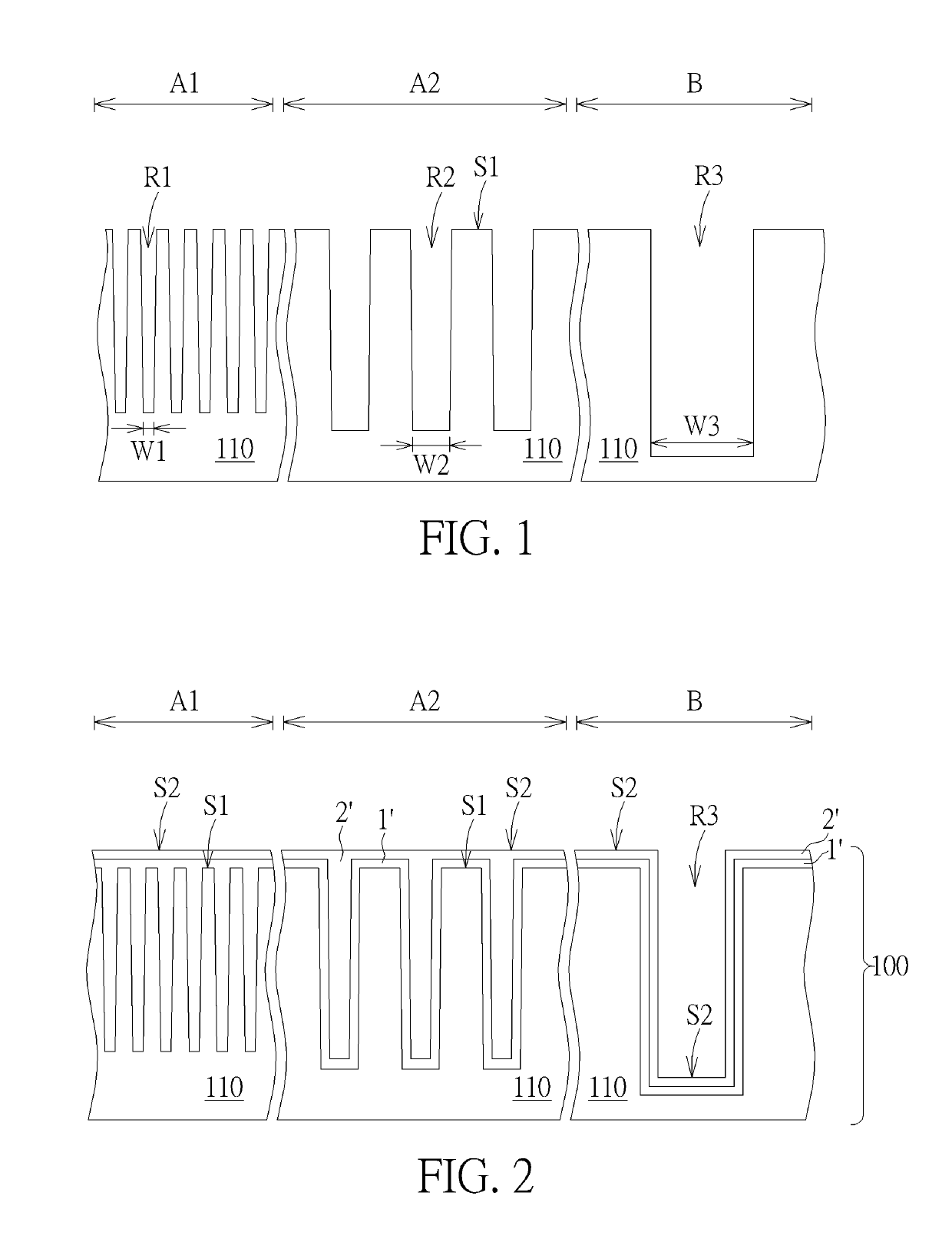
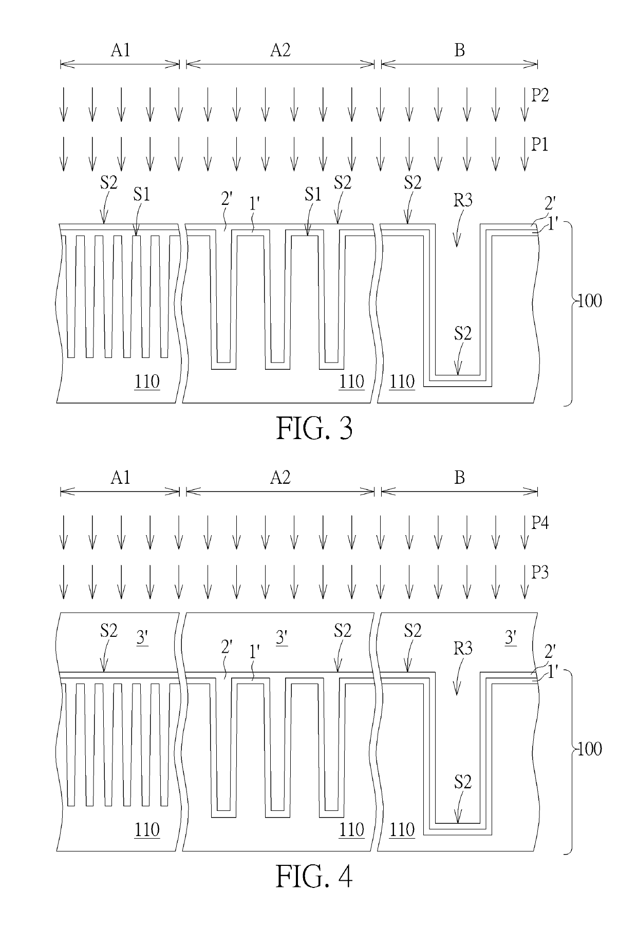
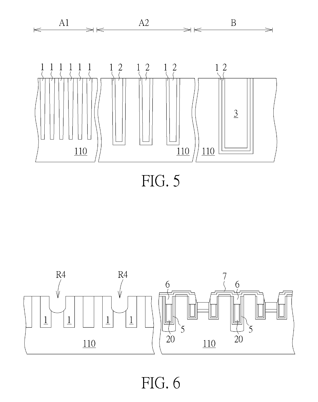
[0012]FIGS. 1-5 schematically depict cross-sectional views of a method of forming an oxide layer according to an embodiment of the present invention. FIGS. 1-5 depict isolations, which are formed by the method of forming an oxide layer of the present invention and are used for separating recessed dynamic random access memory (DRAM) cells from each other, but the present invention is not restricted thereto.

[0013]As shown in FIG. 1, a substrate 110 is provided. The substrate 110 may be a semiconductor substrate such as a silicon substrate, a silicon containing substrate, a III-V group-on-silicon (such as GaN-on-silicon) substrate, a graphene-on-silicon substrate or a silicon-on-insulator (SOI) substrate. The substrate 110 may be divided into a first area A1, a second area A2 and a third area B, depending upon their functions. For instance, the first area A1 and the second area A2 may be memory cell areas while the third area B may be a periphery area, wherein the circuits in the perip...


PUM


Abstract

A method of forming an oxide layer includes the following steps. A substrate is provided. A surface of the substrate is treated to form an oxygen ion-rich surface. A spin-on-dielectric layer is formed on the oxygen ion-rich surface of the substrate. The present invention also provides a method of forming an oxide layer including the following steps. A substrate is provided. A surface of the substrate is treated with a hydrogen peroxide (H2O2) solution or a surface of the substrate is treated with oxygen containing gas, to form an oxygen ion-rich surface. A spin-on-dielectric layer is formed on the oxygen ion-rich surface of the substrate.

Description

BACKGROUND OF THE INVENTION1. Field of the Invention[0001]The present invention relates generally to a method of forming an oxide layer, and more specifically to a method of forming an oxide layer applying a spin-on dielectric (SOD) process.2. Description of the Prior Art[0002]Spin-on dielectric (SOD) processes or chemical vapor deposition (CVD) processes are widely used for depositing dielectrics. Due to flowable dielectrics used in spin-on dielectric (SOD) processes can fill up recesses in a substrate easily by adjusting the solutions of the flowable dielectrics, spin-on dielectric (SOD) process becomes a major way to deposit dielectrics.[0003]For a semiconductor structure, trenches with various sizes are set on a substrate. As the flowable dielectric is spin-coated on the substrate through a spin-on dielectric (SOD) process, the flowable dielectric should fill up the trenches in the substrate. However, the dielectrics formed from the flowable dielectrics would have defects such a...

Claims


Application Information

Patent Timeline
Patent Type & Authority Patents(United States)
IPC IPC(8): H01L21/02H01L21/76H01L21/762H01L27/108
CPCH01L21/76237H01L27/10885H01L27/10897H01L27/10876H01L21/0206H01L27/10823H01L27/10888H01L21/02307H01L21/02337H01L27/10891H01L21/76229H01L21/02312H01L21/02323H01L21/02282H01L27/10894H01L27/10814H10B12/34H10B12/315H10B12/053H10B12/50H10B12/488H10B12/485H10B12/09H10B12/482
Inventor HUANG, CHENG-HSULEE, JUI-MINCHANG, CHING-HSIANGCHEN, YI-WEILIU, WEI-HSINTZOU, SHIH-FANG
Owner FUJIAN JINHUA INTEGRATED CIRCUIT CO LTD
Why Eureka
Try Eureka