Nonvolatile digital computing with ferroelectric FET

a technology of ferroelectric fet and digital computing, which is applied in the direction of digital storage, semiconductor devices, instruments, etc., can solve the problems of limited endurance, limited use of dynamic energy or power, and large energy requirements of conventional nonvolatile memories

Active Publication Date: 2019-11-12
PENN STATE RES FOUND
View PDF8 Cites 1 Cited by
  • Summary
  • Abstract
  • Description
  • Claims
  • Application Information

AI Technical Summary

Benefits of technology

[0008]Any of the NVM devices can have a Fe field effect transistors (FeFET) configured to exploit the IDS-VG hysteresis of the steep switch at low voltage for logic memory synergy. The FeFET-based devices can be configured to include a wide hysteresis, a steep hysteresis edge, and high ratio between the two IDS states at VG=0. This can be achieved by shifting the hysteresis of the FeFET by Vth engineering and tuning other parameters by adjusting the ferroelectric layer thickness and ferroelectric area. In some embodiments, the hysteresis can be shifted to center the hysteresis window around VG=0, which may provide extra non-volatility to the FeFET-based device. Some embodiments can be configured to operate on higher ON-state current and lower OFF-state current to provide faster restore operations, as well as provide immunity to device variations.
[0009]Embodiments of the FeFET-based devices can be used to produce nonvolatile DFFs that maintain their state during power outages. These DFFs, used as nonvolatile memories, can facilitate computing without the loss of computation states during a power failure, which can be achieved by nonvolatile processing techniques of embedding the FeFET-based device on a memory chip so that the FeFET-based device can serve as a logic transistor. In some embodiments, the DFFs can be configured to operate with external backup and restore control signals. In some embodiments, the DFFs can be configured to operate without external backup and restore control signals, which can be achieved by the addition of transistors to the nonvolatile memory cell design. Embodiments of the DFF can be configured to consume negligible static current in backup and in restore operations, be energy efficient, have low latency backup and restore operations, and have low energy-delay overhead.

Problems solved by technology

Conventional nonvolatile memories tend to require a large amount of energy for suitable operation.
The energy consumed during backup and restore operations can be factors that lead to this large energy requirement.
Conventional nonvolatile memories can also be plagued with limited speed, limited endurance, and / or limited use of dynamic energy or power.
Not only can the effects of such limitations result in wasted energy consumption, these and other limitations exhibited by conventional nonvolatile memories may hinder implementation of energy saving techniques.
This inability to implement energy saving techniques can be exacerbated during frequent data access operations when the conventional nonvolatile memory is used as a memory cell during computation and / or logic switching.

Method used


Image

  • Nonvolatile digital computing with ferroelectric FET
  • Nonvolatile digital computing with ferroelectric FET
  • Nonvolatile digital computing with ferroelectric FET

Examples


Embodiment Construction

[0124]The following description is of exemplary embodiments that are presently contemplated for carrying out the present invention. This description is not to be taken in a limiting sense, but is made merely for the purpose of describing the general principles and features of the present invention. The scope of the present invention is not limited by this description.

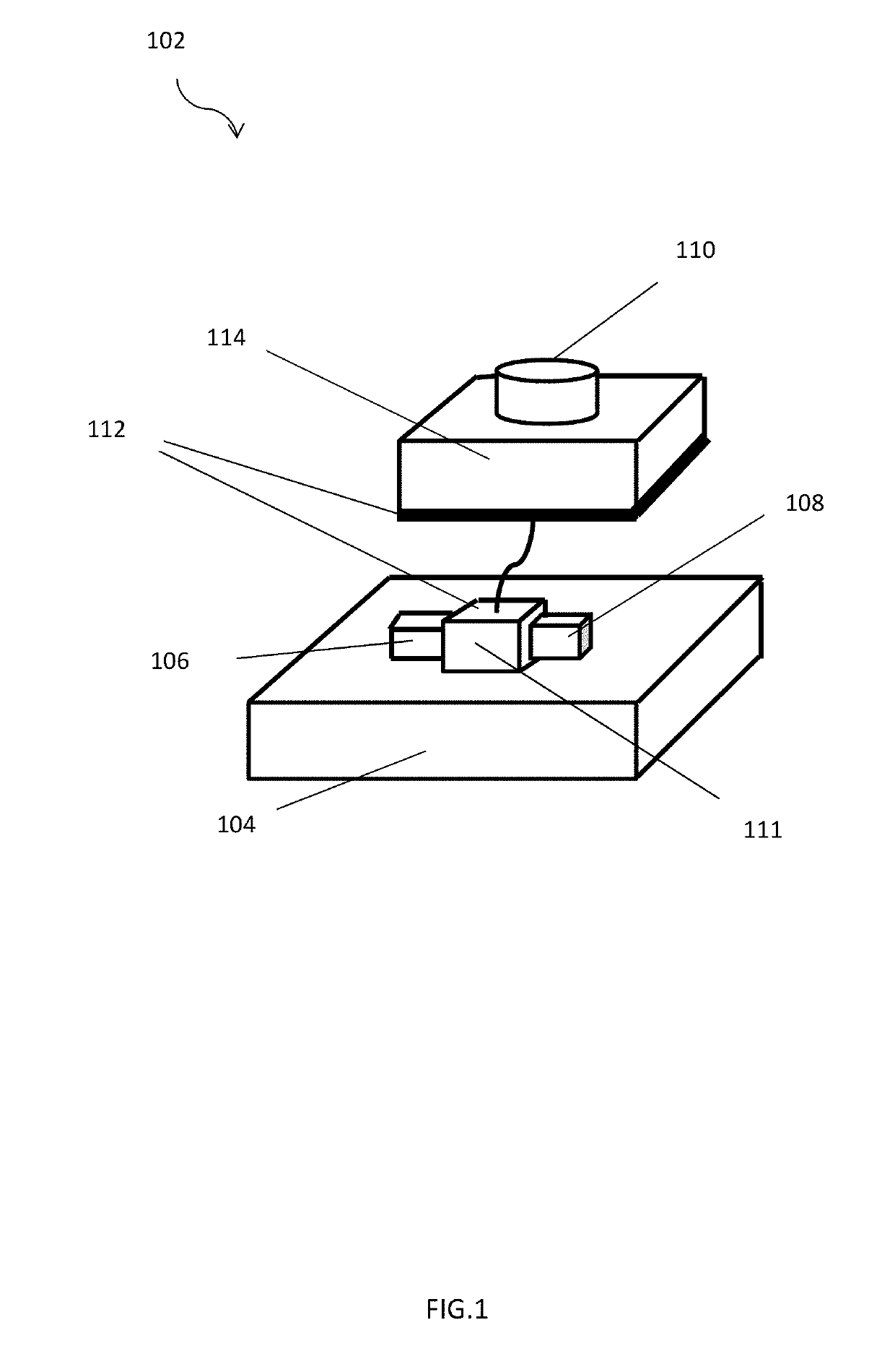
[0125]Embodiments include nonvolatile a memory (NVM) device 100 that can be configured for logic switching and / or digital computing. For example, embodiments of the NVM device 100 can be configured as any one or combination of a memory cell 124, a D flip flop (DFF) 120, a Backup and Restore circuit (B&R circuit) 116, and / or a latch 118, 122 for a DFF 120.

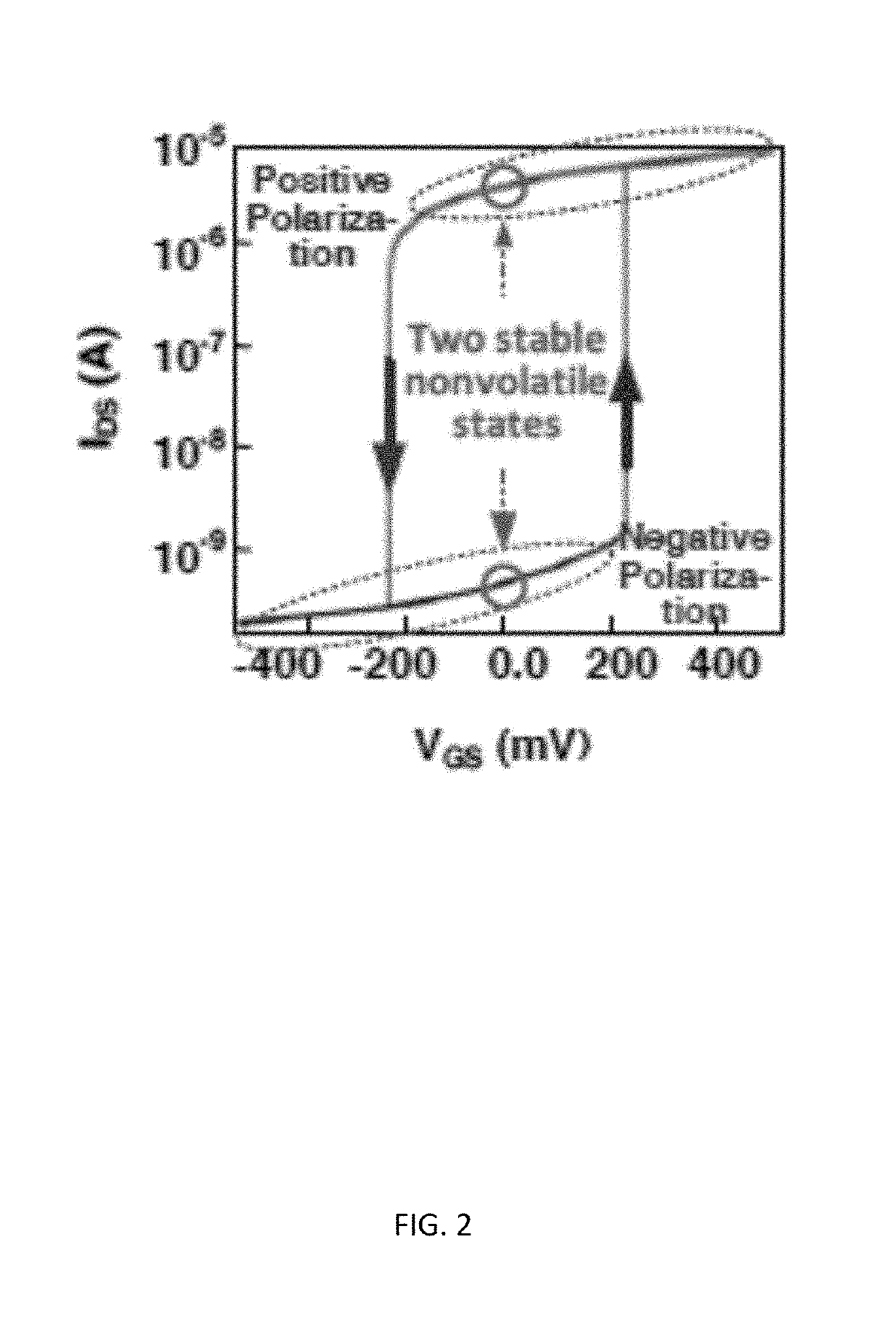
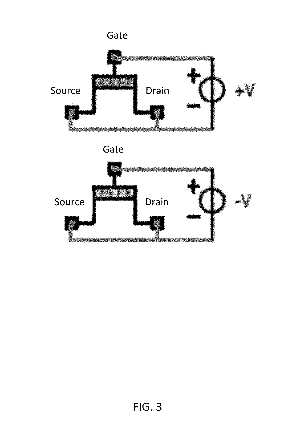
[0126]Referring to FIGS. 1-3, in some embodiments, the NVM device 100 can include at least one field effect transistor (FET) 102. The FET 102 can include a substrate 104 having a drain 106, a source 108, and a gate 110 formed thereon. The drain 106, source 108, and gate...


PUM


Abstract

Embodiments include nonvolatile a memory (NVM) device that can be configured for logic switching and / or digital computing. For example, embodiments of the NVM device can be configured as any one or combination of a memory cell, a D flip flop (DFF), a Backup and Restore circuit (B&R circuit), and / or a latch for a DFF. Any of the NVM devices can have a Fe field effect transistors (FeFET) configured to exploit the IDS-VG hysteresis of the steep switch at low voltage for logic memory synergy. The FeFET-based devices can be configured to include a wide hysteresis, a steep hysteresis edge, and high ratio between the two IDS states at VG=0.

Description

CROSS-REFERENCE TO RELATED APPLICATIONS[0001]This Application is related to and claims the benefit of priority to U.S. Provisional Application Ser. No. 62 / 504,775 filed on May 11, 2017, the entire contents of which is incorporated herein by reference.STATEMENT REGARDING FEDERALLY SPONSORED RESEARCH AND DEVELOPMENT[0002]This invention was made with government support under Grant No. HR0011-13-3-0002 awarded by the Department of Defense / Defense Advanced Research Projects Agency (DARPA). The government has certain rights in the invention.FIELD OF THE INVENTION[0003]Embodiments of the invention relate to nonvolatile a memory (NVM) device that can be configured for logic switching and / or digital computing. For example, embodiments of the NVM device can be configured as any one or combination of a memory cell, a D flip flop (DFF), a Backup and Restore circuit (B&R circuit), and / or a latch for a DFF.BACKGROUND OF THE INVENTION[0004]Conventional nonvolatile memories tend to require a large ...

Claims


Application Information

Patent Timeline
Patent Type & Authority Patents(United States)
IPC IPC(8): G11C14/00G11C11/22G11C11/16H01L29/78G11C13/00
CPCG11C13/0061G11C11/1693G11C13/0069G11C14/009G11C14/0054G11C11/2275G11C13/0007G11C14/0081G11C11/2293H01L29/78391G11C11/1675G11C14/0072G11C11/223G11C13/0002
Inventor LI, XUEQINGGEORGE, SUMITHASAMPSON, JOHNGUPTA, SUMEETDATTA, SUMANNARAYANAN, VIJAYKRISHNANMA, KAISHENG
Owner PENN STATE RES FOUND
Why Eureka
Try Eureka