Eureka AIR delivers breakthrough ideas for toughest innovation challenges, trusted by R&D personnel around the world.

Manufacturing method for EMI shielding structure

a manufacturing method and shielding technology, applied in the direction of cross-talk/noise/interference reduction, non-printed electric components of printed circuits, and semiconductor/solid-state device details, etc., can solve the problems of structure may have a problem, increase the unit price of a product, and reduce the shaping and processing time of the dam. , the effect of increasing the mounting region of the printed circuit board

Active Publication Date: 2019-11-12
SAMSUNG ELECTRONICS CO LTD
View PDF125 Cites 0 Cited by
  • Summary
  • Abstract
  • Description
  • Claims
  • Application Information

AI Technical Summary

Benefits of technology

[0010]One of more exemplary embodiments provide an EMI shielding structure which can omit an interval between adjacent shielding regions, minimize dam shaping and processing time, and increase a mounting region of a printed circuit board, and a manufacturing method thereof.
[0011]One or more exemplary embodiments also provide an EMI shielding structure which can save a material cost by removing use of a shield can and instead forming a shielding structure with shaping and molding, and a manufacturing method using the same.

Problems solved by technology

Therefore, there may be a problem in which the EMI shielding structure including a related art shield can degrade a high integration rate of the circuit devices.
Further, a related art EMI shielding structure may have a problem of causing increased unit price of a product, due to need for separate press processes in the fabrication of the shield cans and for expensive materials used for the shield cans.
Also, an exemplary embodiment is not required to overcome the disadvantages described above, and an exemplary embodiment may not overcome any of the problems described above.

Method used


Image

  • Manufacturing method for EMI shielding structure
  • Manufacturing method for EMI shielding structure
  • Manufacturing method for EMI shielding structure

Examples


Embodiment Construction

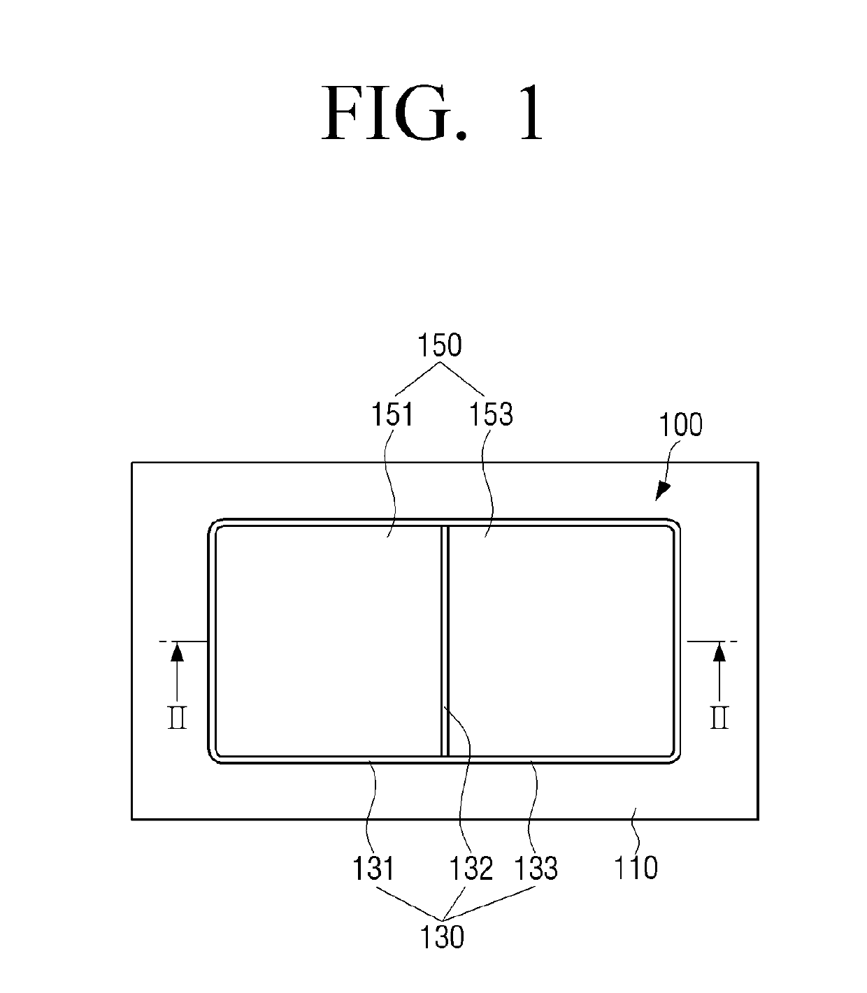
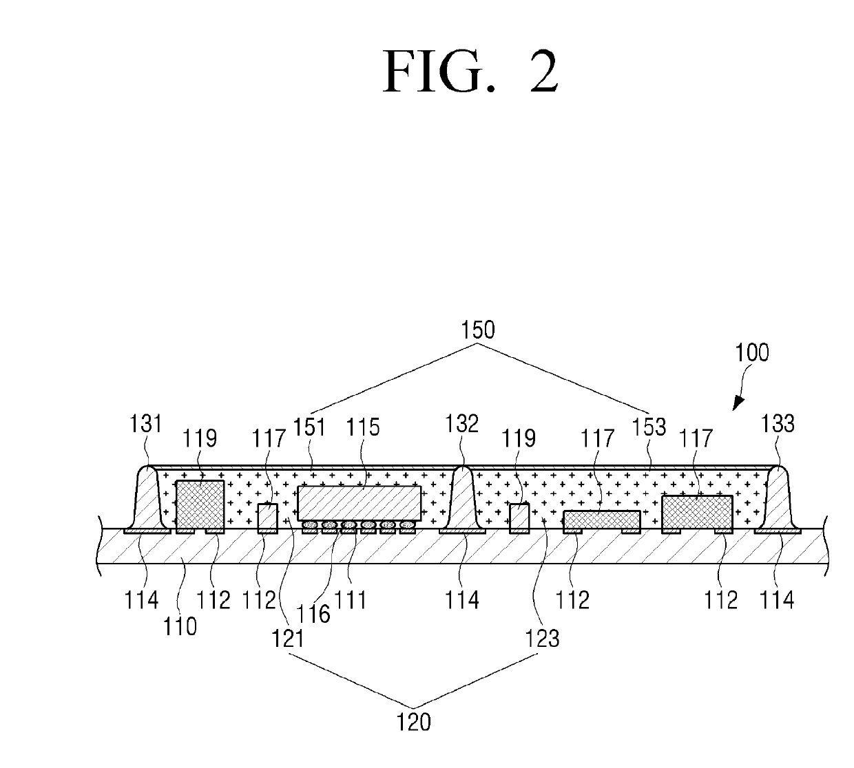
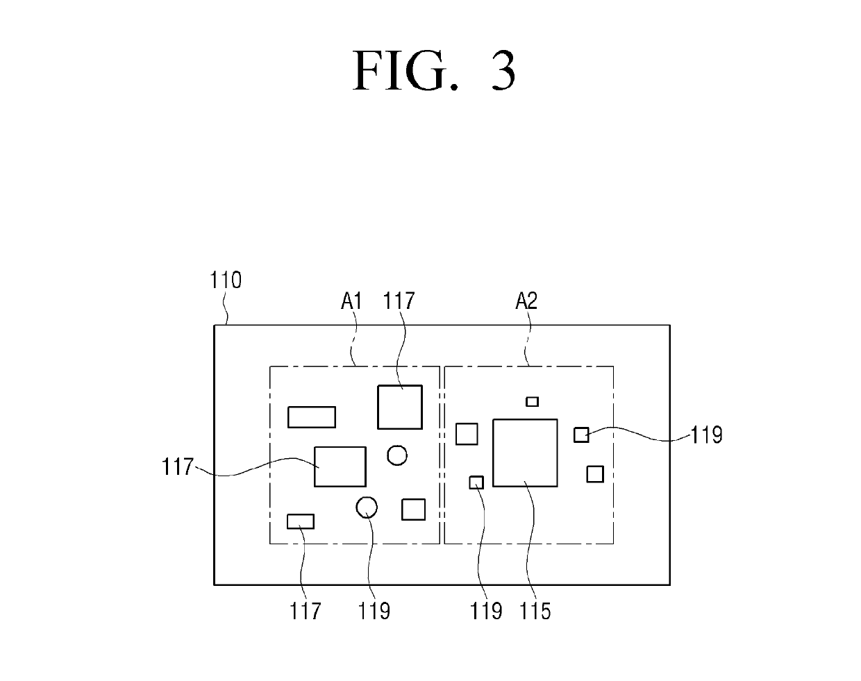
[0054]Certain exemplary embodiments of the present inventive concept will now be described in greater detail with reference to the accompanying drawings.

[0055]In the following description, same drawing reference numerals are used for the same elements even in different drawings. The matters defined in the description, such as detailed construction and elements, are provided to assist in a comprehensive understanding of the present inventive concept. Accordingly, it is apparent that the exemplary embodiments of the present inventive concept can be carried out without those specifically defined matters. Also, well-known functions or constructions are not described in detail since they would obscure the invention with unnecessary detail.

[0056]When an element is stated as being “on” or “in contact with” another element, it is to be understood that the element may be directly contacted or connected with another element, but may also be intervened with yet another element disposed therebe...


PUM


Abstract

An electromagnetic interference (EMI) shielding structure and a manufacturing method thereof are provided. The EMI shielding structure includes a shielding dam provided on a printed circuit board, the shielding dam forming a closed loop that defines a periphery of adjacent shielding regions of the printed circuit board; an insulating member that is provided on the adjacent shielding regions within the shielding dam, the insulating member covering circuit devices provided in the adjacent shielding regions; and a shielding member that covers an upper surface of the insulating member, wherein the shielding dam includes a border portion surrounding the adjacent shielding regions, and a partition portion disposed between the adjacent shielding regions and within the border portion.

Description

CROSS-REFERENCE TO RELATED APPLICATIONS[0001]This application claims priority from U.S. Provisional Application No. 62 / 370,781, filed on Aug. 4, 2016 in the United States Patent and Trademark Office, and Korean Patent Application No. 10-2016-0154190, filed on Nov. 18, 2016 in the Korean Intellectual Property Office, the disclosures of which are incorporated herein by reference in their entirety.BACKGROUND[0002]1. Field of the Invention[0003]Apparatuses and methods consistent with exemplary embodiments relate to an electromagnetic interference (EMI) shielding, and more particularly, to an EMI shielding structure configured to increase a mounting region of a printed circuit board by removing intervals between adjacent shielding regions, and a manufacturing method of the EMI shielding structure.[0004]2. Description of the Related Art[0005]Demands for mobile devices have rapidly increased in the recent electronic product market, and also, it is continuously demanded that the mobile devi...

Claims


Application Information

Patent Timeline
Patent Type & Authority Patents(United States)
IPC IPC(8): H05K1/00H01L23/552H05K1/18H05K9/00H05K1/02B05D1/26B05D7/00
CPCH05K9/0024H01L23/552H05K1/182H05K1/0218H05K2203/0126B05D7/50H01L2924/19105H05K2201/10204H01L2924/19041B05D1/26H01L2924/19043H01L2924/3025H01L2924/19042H05K2201/09972H01L2224/16227
Inventor MUN, IL-JUKUK, KEONYEOM, JI-WOON
Owner SAMSUNG ELECTRONICS CO LTD
Why Eureka
Eureka Blog
Learn More