Method for processing silicon material

a technology of silicon material and processing method, which is applied in the field of treating a semiconductor material, can solve the problems of complexes that can form electrically active defects, reduce performance, and only apply techniques to defects already present in silicon, and achieve rapid stabilisation of the bulk life of silicon material, improved structure performance, and high injection of majority carriers

Active Publication Date: 2019-12-10
NEWSOUTH INNOVATIONS PTY LTD
View PDF4 Cites 0 Cited by
  • Summary
  • Abstract
  • Description
  • Claims
  • Application Information

AI Technical Summary

Benefits of technology

[0023]In embodiments, the cooled temperature is such to minimise reactivation of passivated defects.
[0055]The methods of the first and second aspects may be selectively applied to a localised portion of a silicon device to improve the performance of a structure disposed at the localised portion.
[0056]Advantageous embodiments of the present invention provide a method for rapidly stabilising the bulk lifetime of silicon material, for example in a silicon solar cell. This is achieved through a deliberate and accelerated formation of electrically active defects and hydrogen passivation of electrically active defects. The method uses a very high intensity light (higher than 3 suns) to provide very high injection of majority carriers in the silicon. The same light is used to control the temperature of the silicon during the process in order to accelerate and optimise the defect formation and passivation processes. In particular, in some embodiments the temperature of the silicon is controlled by providing light with an alternate waveform and varying the frequency of the waveform. Temperature control can be facilitated by using thermal masses, which can be moved into contact, or out of contact with the silicon material.
[0057]The synergy between the very high intensity light and the temperature control provide the ability to achieve a 90% or better stabilisation of the silicon material in an extremely short period of time. In some embodiments this period of time is shorted than 5 seconds.

Problems solved by technology

These complexes can form electrically active defects when exposed to radiation, such as visible light.
Electrically active defects throughout a solar cell affect the lifetime of charge carriers causing reduced performance.
However these techniques only apply to defects that are already present in the silicon.
Thus any defects that form subsequent to this processing will still adversely impact the solar cell efficiency.
P-type Czochralski (Cz) silicon solar cells, for example, are known to suffer from light induced degradation (LID) which may causes a drop in efficiency of up to 3% absolute during the first 24-48 hours of operation.
Similarly polycrystalline silicon solar cells have been shown to suffer from a similar light induced degradation in performance, although on a much slower timescale compared to Cz wafers.
Thus in general these techniques require hours or even days to stabilise the silicon material.
This is generally incompatible with the high throughput solar cell manufacturing environment.

Method used


Image

  • Method for processing silicon material
  • Method for processing silicon material
  • Method for processing silicon material

Examples


Embodiment Construction

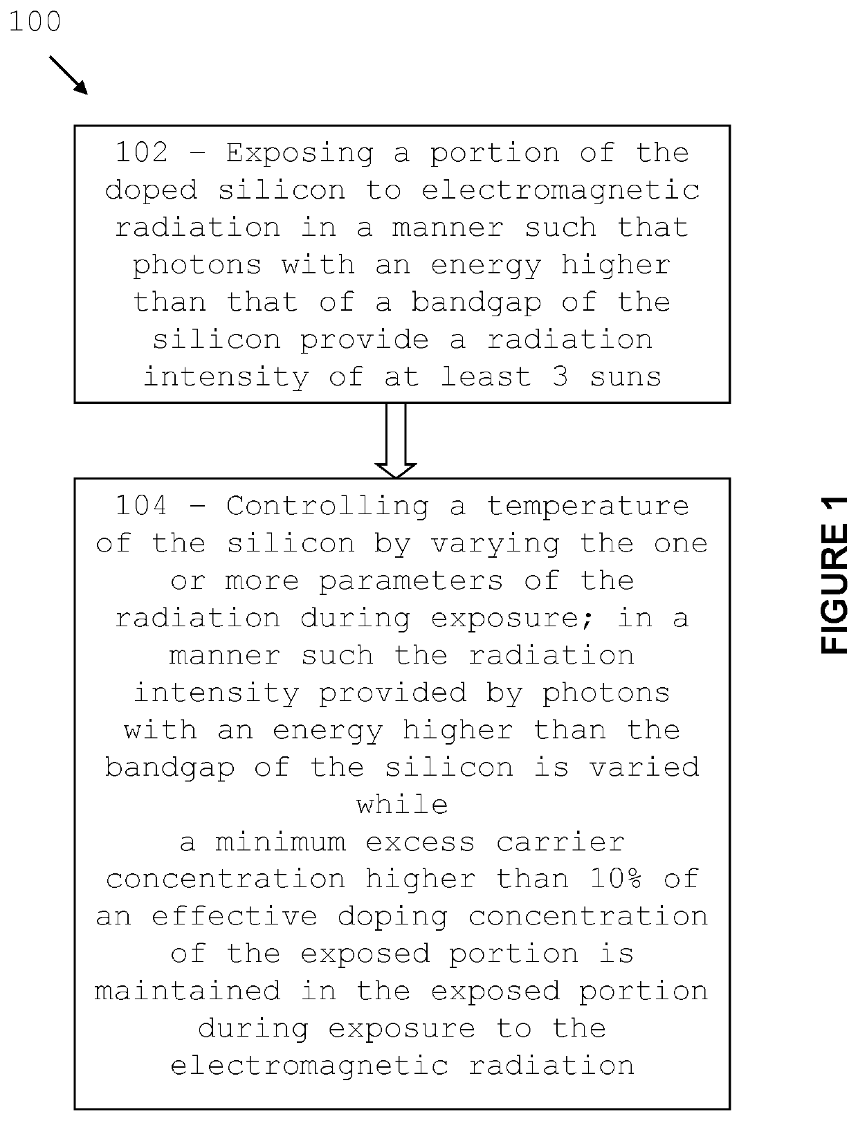
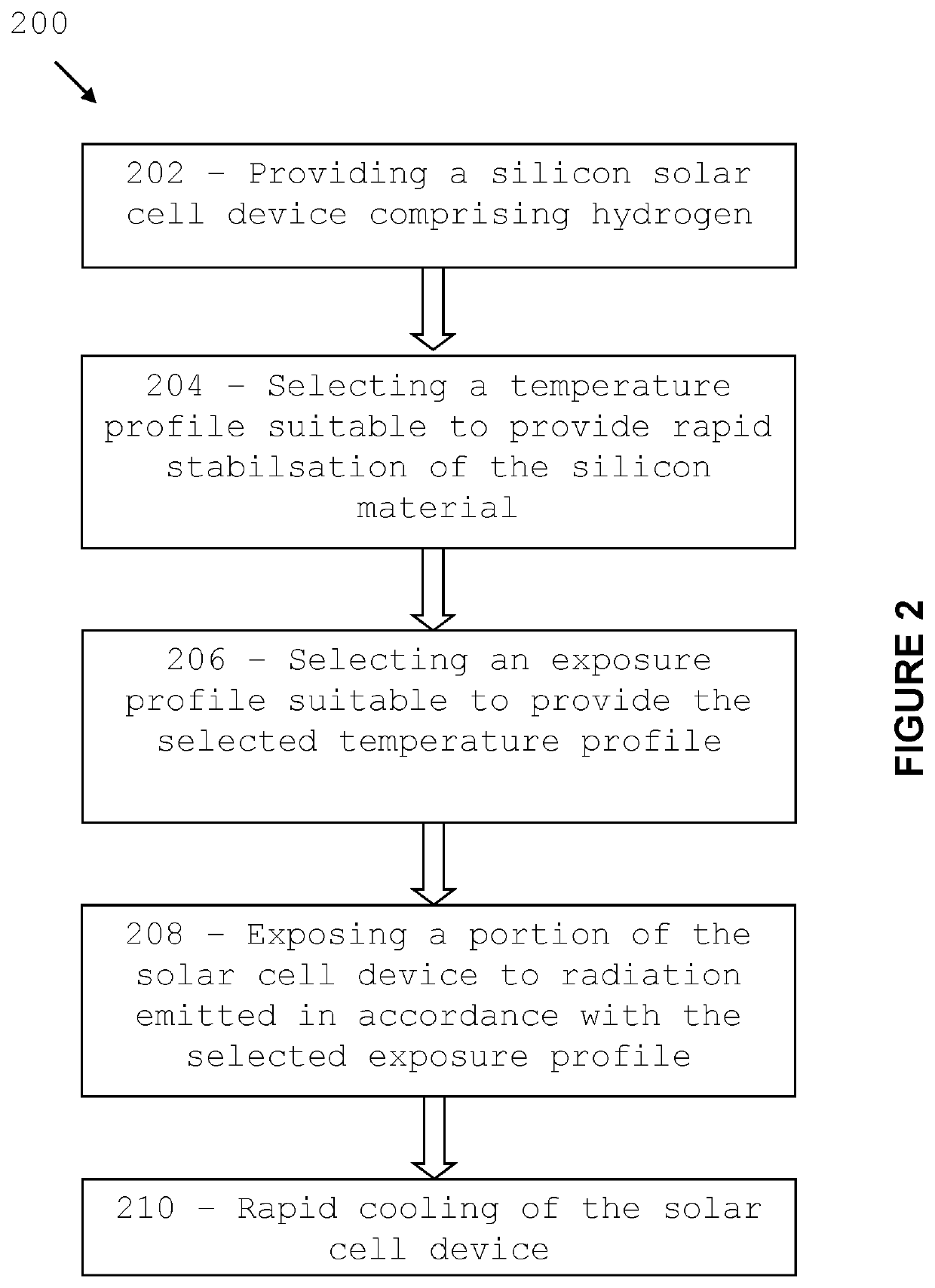
[0068]Embodiments of the present invention relate to a method for rapidly stabilising the lifetime of minority carrier in doped silicon material by a deliberate and accelerated formation of electrically active defects and passivation of the defects. The silicon material is exposed to a high intensity radiation. The radiation is absorbed in the silicon material and generates excess minority and majority carriers. In addition, the radiation provides thermal energy to control the temperature of the silicon during the stabilisation process.

[0069]The exposure to high intensity radiation and the temperature regimes provided in accordance to embodiments of the invention allow the rapid formation and passivation of electrically defects related to the boron-oxygen complex. A portion of these defects typically has not formed yet when the fabrication of the solar cell is completed. These defects may form when the solar cell is operating in the field—light induced degradation (LID)—causing a dr...


PUM


Abstract

The present disclosure provides a method for accelerating the formation of defects in doped silicon. A doped silicon area is exposed with high intensity electromagnetic radiation to provide a substantial excess of majority carriers and promote a high rate of defect formation to allow efficient silicon passivation.

Description

FIELD OF THE INVENTION[0001]The present invention generally relates to a method for treating a semiconductor material comprising doped silicon. In particular, the invention relates to a method for forming electrically active defects in silicon solar cells and passivating electrically active defects.BACKGROUND OF THE INVENTION[0002]Silicon is the main semiconductor material used to fabricate today's commercial solar cells. The majority of commercial solar cells are fabricated from a monocrystalline or polycrystalline silicon wafer. A p-n junction is formed in the silicon wafer by, for example, diffusing n-type atoms in a p-type silicon wafer.[0003]A large amount of solar cells are fabricated using a boron doped wafer (p-type). The boron atoms introduced in the silicon material tend to form boron-oxygen (B—O) complexes. These complexes can form electrically active defects when exposed to radiation, such as visible light. Similarly polycrystalline wafers are known to contain a wide var...

Claims


Application Information

Patent Timeline
Patent Type & Authority Patents(United States)
IPC IPC(8): H01L21/00H01L31/18
CPCH01L31/1868H01L31/1804H01L31/186Y02E10/547H01L31/068Y02P70/50H01L31/036
Inventor HALLAM, BRETT JASONWENHAM, STUART ROSSABBOTT, MALCOLM DAVIDHAMER, PHILLIP GEORGE
Owner NEWSOUTH INNOVATIONS PTY LTD
Why Eureka
Try Eureka