High concentration doping in silicon

a technology of silicon and doping concentration, applied in the field of high concentration doping in silicon, can solve the problems of reducing the efficiencies of solar cells made from such materials, reducing the minority carrier lifetime of silicon, and unsatisfactory designs of commercially manufactured solar cell structures, so as to reduce the likelihood of reactivation of the dopant atom

Active Publication Date: 2018-04-17
NEWSOUTH INNOVATIONS PTY LTD
View PDF12 Cites 2 Cited by
  • Summary
  • Abstract
  • Description
  • Claims
  • Application Information

AI Technical Summary

Benefits of technology

[0019]Some or all of the deactivated dopant atoms may subsequently be reactivated by subjecting the doped crystalline silicon region to heat in the presence of illumination whereby electron hole pairs are generated to increase the proportion of minority carriers in the doped crystalline silicon region to allow at least some of the released hydrogen atoms to take on a charge state that allows it to escape from the coulombic attraction of the dopant atom to which it was previously bonded. Subsequent cooling of the doped crystalline silicon region while preferably maintaining illumination, minimises the likelihood of the dopant atom being reactivated by hydrogen atoms.
[0020]Some or all of the deactivated dopant atoms in a selected crystalline silicon region may also be subsequently reactivated by subjecting the dopant atoms in the selected crystalline silicon region to heat and illuminating a crystalline silicon region adjacent to the selected region whereby electron hole pairs are generated to increase the proportion of minority carriers in the crystalline silicon region adjacent to the selected crystalline silicon region such that the minority carriers generated in the crystalline silicon region adjacent to the selected crystalline silicon region will diffuse to the selected crystalline silicon region and therefore allow reactivation of the dopants in the selected crystalline silicon region. Again allowing the selected crystalline silicon region to cool to below 120° C. will prevent the dopants from being deactivated again if the minority earners continue to diffuse from the adjacent crystalline silicon region. The heating and / or illumination of the dopant atoms and / or the selected crystalline silicon region and the crystalline silicon region adjacent to the selected crystalline silicon region may be performed with a laser. The laser may be scanned over a plurality of crystalline silicon regions to process a larger area or an entire cell.
[0022]For hydrogen sources external to the silicon, such as dielectric layers, the method will be more effective when silicon surface n-type diffused layers through which hydrogen must diffuse have peak net active doping concentrations (i.e. dopant atoms that have not been deactivated) of 1×10²⁰ atoms / cm3 or less. Similarly, the method will be more effective when any silicon surface diffused p-type layers through which hydrogen must diffuse have peak net active doping concentrations of 1×10¹⁹ atoms / cm3 or less.
[0026]Minority carrier concentrations may be controlled, through the use of light and heat, during a cool-down period after heating, and any post hydrogenation thermal processes, to maintain hydrogen charge states during cool-down to minimise reactivation of defects, or reactivation of dopants, to which hydrogen atoms have previously bound.

Problems solved by technology

These lower the minority carrier lifetime of the silicon and therefore reduce the efficiencies of solar cells made from such material.
Currently, without a full understanding of the hydrogenation process and its potential, the designs of commercially manufactured solar cell structures are not ideal to facilitate hydrogenation throughout the cell, and this is reflected in the poor bulk lifetimes for technologies using standard commercial grade p-type wafers.
However hydrogen in these charge states in the respective silicon polarity can lead to strong attraction between the hydrogen atom and the respective dopant atoms, making it difficult for the hydrogen atom to move past such dopant atoms.
This behaviour of hydrogen in silicon has not been well understood or has been overlooked in the past, with the result that attempts at hydrogenation have been less effective than would have been believed by cell designers.
The dissociation of the dopant-hydrogen complexes is difficult, as even if there is sufficient thermal energy to dissociate the complex (e.g. >150° C.
It can now be seen that the main reasons for poor hydrogenation in the past include: heavy doping in emitters blocking hydrogen from penetrating deep within the silicon; absence of hydrogen sources from one or both surfaces; aluminium alloyed regions or metal / silicon interfaces acting as sinks; failure to achieve the right charge state, for the atoms of hydrogen to facilitate their bonding to certain types of defects and impurities; and no means of trapping of the hydrogen.

Method used


Image

  • High concentration doping in silicon
  • High concentration doping in silicon
  • High concentration doping in silicon

Examples


examples

1. Deliberate Addition of Extra Boron (B) and Subsequent Deactivation by Hydrogen in Localised Areas to Form a Selective Emitter

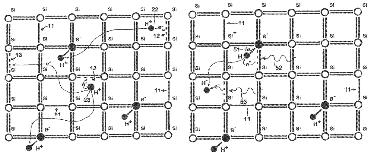
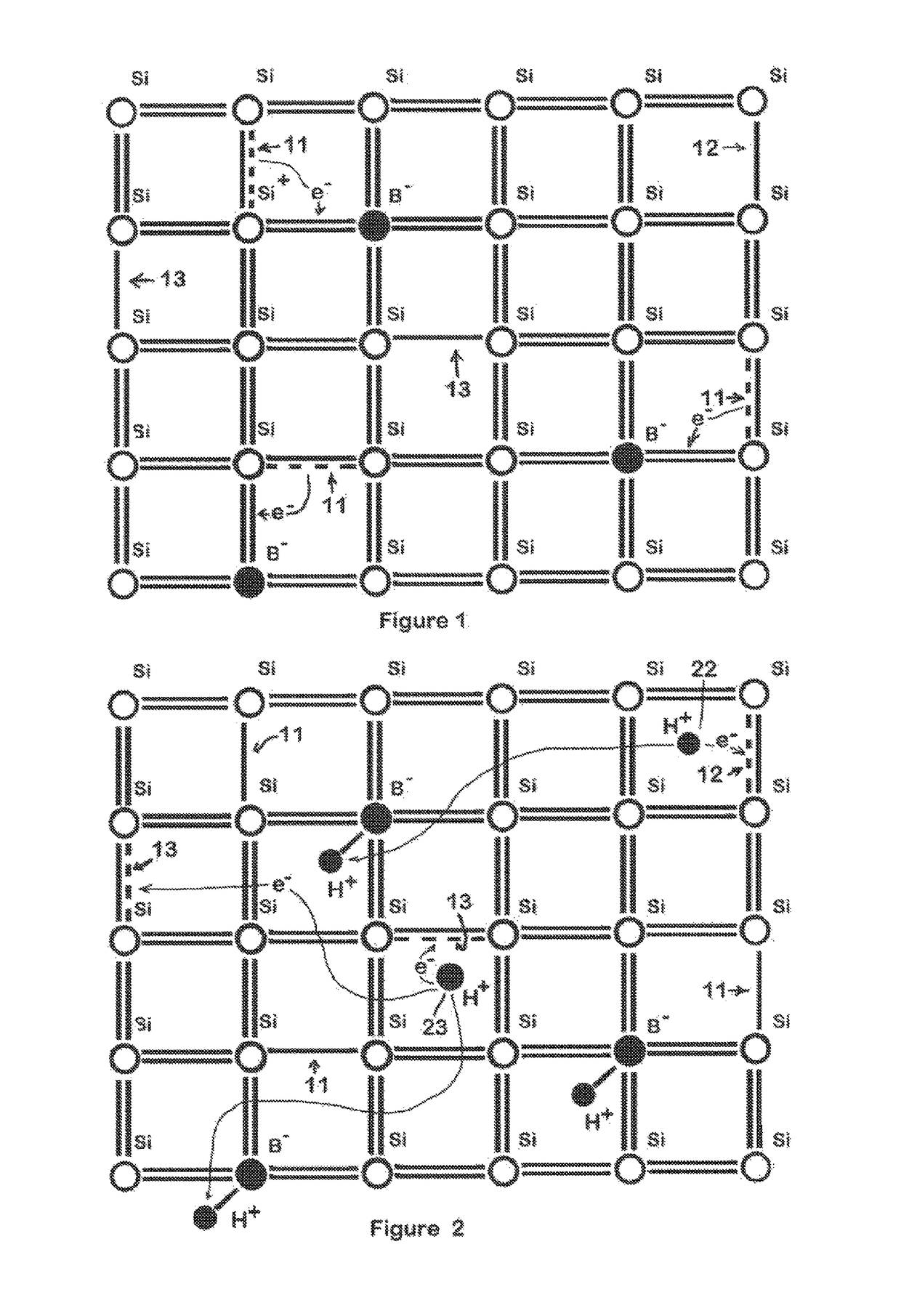
[0074]Boron (or other dopants) can be intentionally added to the silicon. By manipulating the charge state of hydrogen in some or all areas of the device and providing sufficient thermal energy (typically 150°-500° C.) to increase the amount and mobility of the hydrogen, the boron can be de-activated (or re-activated as desired)—by enabling boron & hydrogen to bond together (or break and separate if boron reactivation is desired). This has many important implementations such as profiling resistivity in an emitter to form a selective Emitter, which can be done in a number of ways including but not limited to:

(i) Example 1—Local Deactivation

1) Referring to FIG. 7, an n-type wafer 70 is textured 71;

2) A boron diffusion of the top surface to notionally achieve a p+ region with a sheet resistance of 45-55Ω / □ (but which could be anywhere within a range of 1-80Ω / □...

example 2

(ii) Local Deactivation

1) Referring to FIG. 16, a p-type wafer 160 is textured 161;

2) A phosphorus diffusion of the top surface to notionally achieve an n+ region with a sheet resistance of 45-55Ω / □ (but which could be anywhere within a range of 1-80Ω / □) creates an emitter layer 172 seen in FIG. 17;

3) A boron diffusion 173 may also be added to the rear surface to again notionally achieve an p− region with a sheet, resistance of 45-55Ω / □ (but which could be anywhere within a range of 1-80Ω / □) as also seen in FIG. 17;

[0077]4) A front surface dielectric layer 183 and a rear surface dielectric layer 184 are then deposited as seen in FIG. 18. The dielectric layers 183&184 act as hydrogen sources and may be selected from hydrogen containing dielectric materials such as silicon nitride, silicon oxynitride, aluminium oxides etc.;

5) The front surface dielectric layer 183 is patterned as seen in FIG. 19, to create openings 195 for emitter metallisation. This can be done by a laser 191, by scr...

example 3

(iii) Deactivation and Local Reactivation

[0078]1) Referring to FIG. 25, hydrogenation is performed on a n-type wafer 70 similar to that see in FIG. 9 to produce a lightly doped emitter layer 252 prior to patterning of the top surface dielectric 93. This process manipulates the charge state in such a way that boron is deactivated wherever hydrogen is present. Boron is deactivated by hydrogen (H+) which bonds with the negative boron atoms that are active in the silicon lattice. Hydrogenation performed in a manner which maximises the amount of H+ present will enable the H+ to bond with the B− thereby de-activating the boron and creating higher sheet resistivity material in these regions. As there is no patterning of the dielectric layer 93 there will be no remaining lower sheet resistivity regions 82. Note that, as before, the percentage of atomic hydrogen in the positive charge state is maximised by keeping the electron concentration low such as by minimising any light having photons ...


PUM


Abstract

A silicon device, has a plurality of crystalline silicon regions. One crystalline silicon region is a doped crystalline silicon region. Deactivating some or all of the dopant atoms in the doped crystalline silicon region is achieved by introducing hydrogen atoms into the doped 5 crystalline silicon region, whereby the hydrogen coulombicly bonds with some or all of the dopant atoms to deactivate the respective dopant atoms. Deactivated dopant atoms may be reactivated by heating and illuminating the doped crystalline silicon region to break at least some of the dopant-hydrogen bonds while maintaining conditions to create a high concentration of neutral hydrogen atoms whereby 10 some of the hydrogen atoms diffuse from the doped crystalline silicon region without rebinding to the dopant atoms.

Description

INTRODUCTION[0001]The present invention relates to methods of manufacturing solar cells and in particular the invention provides new method of hydrogenation of silicon material.BACKGROUND[0002]Hydrogenation of crystalline silicon involves the bonding of hydrogen atoms to crystallographic defects or contamination within, the silicon lattice in a way that prevents that defect or contaminant from acting as a recombination site for minority charge carriers. This is known as passivation of the particular recombination site. This is important for semiconductor devices that require long minority carrier lifetimes such as solar cells and particularly where cheap silicon is used that often has poor crystallographic quality and / or purity and therefore needs passivation to bring the quality to acceptable levels for high efficiency solar cells.[0003]Low cost silicon in general has much higher densities of silicon crystallographic defects and / or unwanted impurities. These lower the minority carr...

Claims


Application Information

Patent Timeline
Patent Type & Authority Patents(United States)
IPC IPC(8): H01L21/324H01L21/225H01L21/30H01L31/068H01L21/22H01L31/18H01L31/0288H01L31/0352
CPCH01L31/068H01L21/2225H01L21/2255H01L21/3003H01L21/324H01L31/0288H01L31/1804H01L31/186H01L31/1864H01L31/1876H01L31/035272Y02P70/521Y02E10/547Y02P70/50
Inventor HALLAM, BRETT JASONEDWARDS, MATTHEW BRUCEWENHAM, STUART ROSSHAMER, PHILLIP GEORGECHAN, CATHERINE EMILYCHONG, CHEE MUNLU, PEI HSUANMAI, LYSONG, LI HUISUGIANTO, ADELINEWENHAM, ALISON MAREEXU, GUANG QI
Owner NEWSOUTH INNOVATIONS PTY LTD
Why Eureka
Try Eureka