Thermal processing in silicon
a technology of silicon and thermal processing, applied in the direction of sustainable manufacturing/processing, semiconductor/solid-state device details, final product manufacturing, etc., can solve the problems of low minority carrier lifetime of silicon, reduced efficiencies of solar cells made from such materials, and unsatisfactory design of commercially manufactured solar cell structures
- Summary
- Abstract
- Description
- Claims
- Application Information
AI Technical Summary
Benefits of technology
Problems solved by technology
Method used
Image
Examples
example 1
ctivation
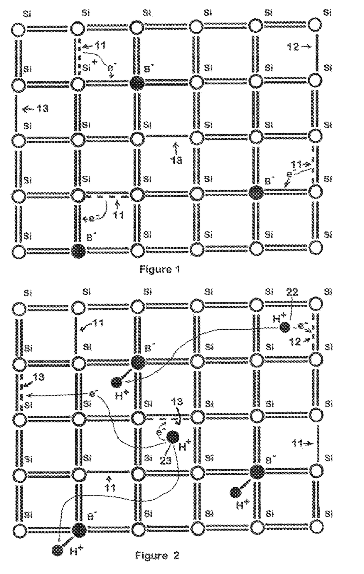
[0087]Boron (or other dopants) can be intentionally added to the silicon. By manipulating the charge state of hydrogen in some or all areas of the device and providing sufficient thermal energy (typically 150°-500° C.) to increase the amount and mobility of the hydrogen, the boron can be de-activated (or re-activated as desired)—by enabling boron & hydrogen to bond together (or break and separate if boron reactivation is desired). This has many important implementations such as profiling resistivity in an emitter to form a selective Emitter, which can be done in a number of ways including but not limited to:
1) Referring to FIG. 7, an n-type wafer 70 is textured 71;
2) A boron diffusion of the top surface to notionally achieve a p+ region with a sheet resistance of 45-55Ω / □ (but which could be anywhere within a range of 1-80Ω / □) creates an emitter layer 82 seen in FIG. 8;
3) A phosphorus diffusion 93 may also be added to the rear surface to again notionally achieve an n+ regio...
example 2
(ii) Local Deactivation
1) Referring to FIG. 16, a p-type wafer 160 is textured 161;
2) A phosphorus diffusion of the top surface to notionally achieve an n+ region with a sheet resistance of 45-55Ω / □ (but which could be anywhere within a range of 1-80Ω / □) creates an emitter layer 172 seen in FIG. 17;
3) A boron diffusion 173 may also be added to the rear surface to again, notionally achieve an p− region with a sheet resistance of 45-55Ω / □ (but which could be anywhere within a range of 1-80Ω / □) as also seen in FIG. 17;
[0091]4) A front surface dielectric layer 183 and a rear surface dielectric layer 184 are then deposited as seen in FIG. 18. The dielectric layers 183&184 act as hydrogen sources and may be selected from hydrogen containing dielectric materials such as silicon nitride, silicon oxynitride, aluminium oxides etc.;
5) The front surface dielectric layer 183 is patterned as seen in FIG. 19, to create openings 195 for emitter metallisation. This can be done by a laser 191, by scr...
PUM
| Property | Measurement | Unit |
|---|---|---|
| temperature | aaaaa | aaaaa |
| temperature | aaaaa | aaaaa |
| temperature | aaaaa | aaaaa |
Abstract
Description
Claims
Application Information


