Column line clamp circuit for imaging array

a technology of column clamp circuit and imaging array, which is applied in the field of column readout circuit for cmos imaging array and to voltage clamp circuit, can solve the problems of signal loss, precision errors in column clamp voltage set, and conventional column clamp circuits tend to be relatively slow, so as to increase the exposure or brightness of the object reflected

Active Publication Date: 2019-12-31
FOVEON
View PDF26 Cites 2 Cited by
  • Summary
  • Abstract
  • Description
  • Claims
  • Application Information

AI Technical Summary

Benefits of technology

[0012]According to one aspect of the present invention, the clamp circuit is based on Replicate biasing circuit which is a method to ensure that the bias current in the active circuit matches very closely with the bias current in the replicate circuit over process, voltage and temperature variations. This will ensure that Vcolumn=VRColClampFB, where VRColClampFB is set to the desired clamp voltage. The close loop regulator operational amplifier has a feedback path via VRColClampFB which ensures that clamped voltage at column matches very closely to the desired set value Vref. This configuration provides higher precision and speed compared to conventional column voltage clamp implementations. The precision is due to the low gain error set by the high open loop gain of the operational amplifier and high speed is determined by high unity gain bandwidth of the amplifier.

Problems solved by technology

These variations result in precision errors in the column clamp voltage set by the clamp circuit 26.
Such high clamp voltage variations can present a significant problem in image sensors since the bright level signal swing cannot be guaranteed to remain linear or have monotonic behavior that remains within the clipping range of the analog-to-digital converter used to convert the column output signal.
In addition, conventional column clamp circuits tend to be relatively slow and incur signal loss since they are based on open loop systems.
This also presents a problem in image sensors when it is desired to operate them at frame rates suitable for video applications.

Method used


Image

  • Column line clamp circuit for imaging array
  • Column line clamp circuit for imaging array
  • Column line clamp circuit for imaging array

Examples


Embodiment Construction

[0021]Persons of ordinary skill in the art will realize that the following description of the present invention is illustrative only and not in any way limiting. Other embodiments of the invention will readily suggest themselves to such skilled persons.

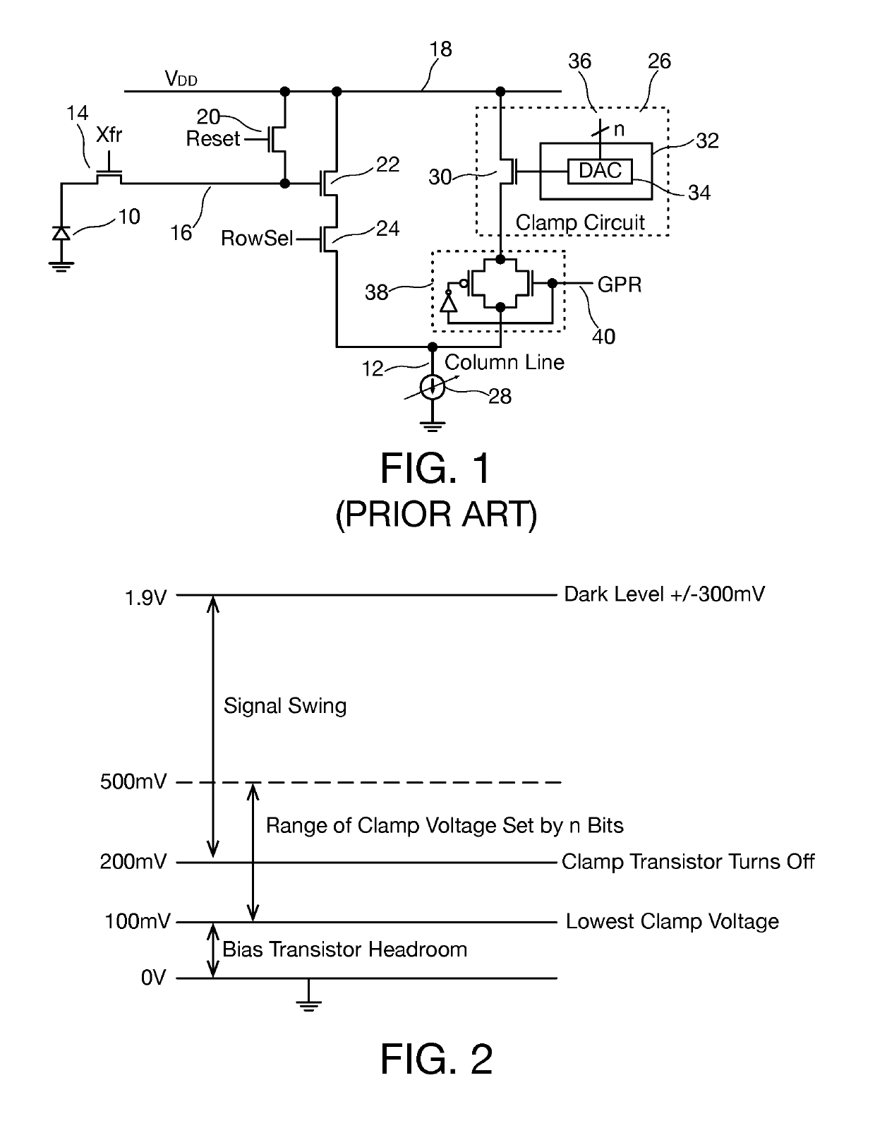
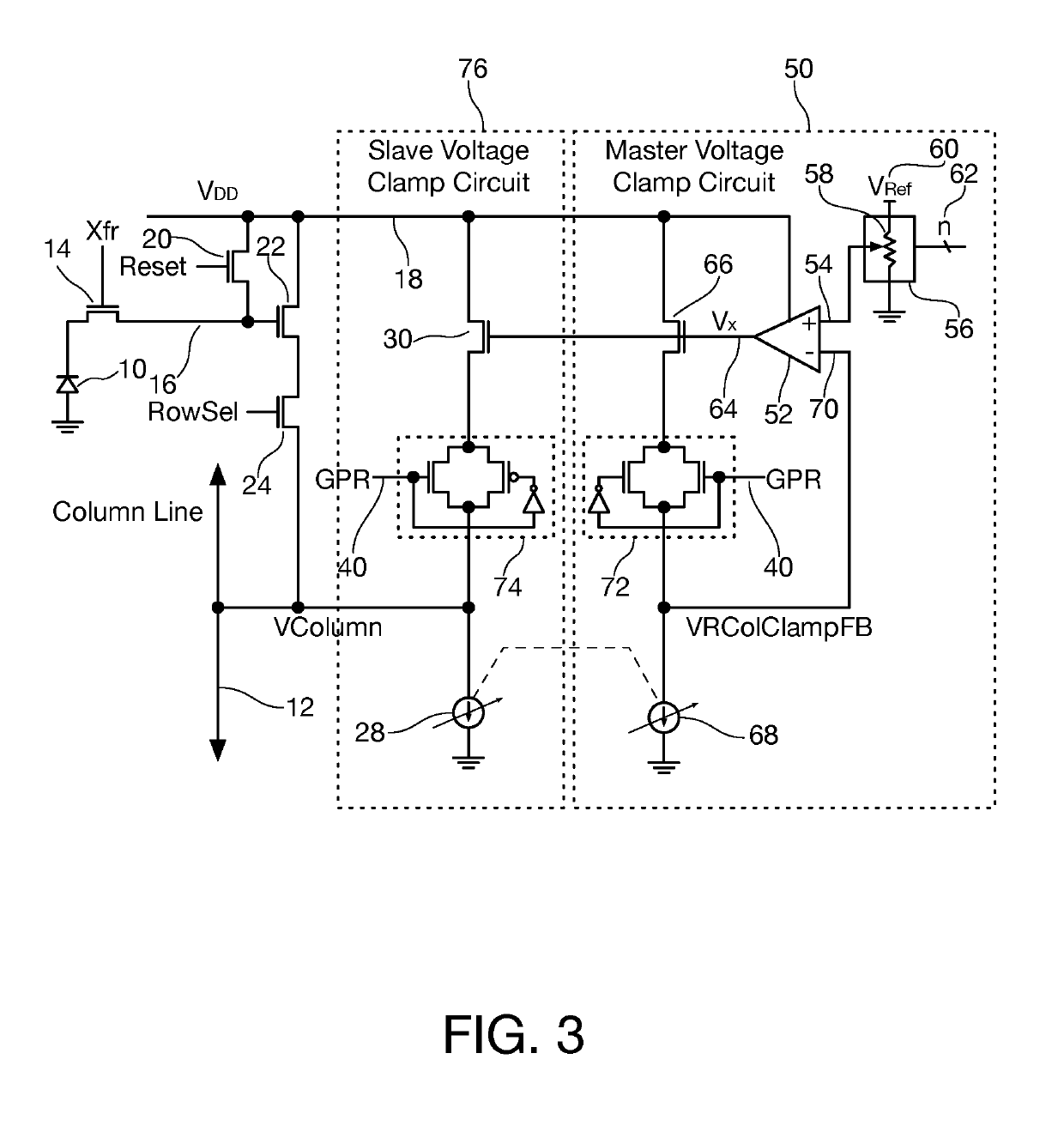
[0022]Referring now to FIG. 3, a column line master voltage clamp circuit 50 in accordance with the present invention is shown. FIG. 3 is a schematic diagram that depicts a typical pixel sensor (photodiode 10) coupled to a column line 12 for reading out the sensed light. A transfer switch 14, usually in the form of an n-channel transistor isolates the photodiode 10 from a floating node 16. The floating node 16 and the cathode of the photodiode 10 are reset to a voltage VDD on line 18 by turning on a reset transistor 20 for a reset period of time while the transfer switch 14 is turned on. After the reset time has ended, reset transistor 20 is turned off and photocharge generated by the photodiode 10 accumulates as a voltage on the capa...


PUM


Abstract

In an imaging array having a plurality of pixel sensors arranged in a plurality of rows and columns, pixel data being read out on column lines of the array, a column line voltage clamp circuit for column lines of the array includes a master voltage clamp circuit coupled to provide a reference voltage clamp level on a reference node, and a slave voltage clamp circuit coupled to each column line in the imaging array, each slave voltage clamp circuit configured to clamp voltage on the column line to a column voltage clamp level derived from the reference voltage level.

Description

BACKGROUND[0001]The present invention relates to CMOS imaging arrays. More particularly, the present invention relates to column readout circuits for CMOS imaging arrays and to voltage clamp circuits for column line readout circuits.[0002]In image sensor circuit, the node voltage on the floating diffusion node drops with increased exposure or brightness level. This voltage drop is reflected in the column voltage when the row select transistor is turned on. A clamp circuit is provided on the column line to define the lowest voltage to which the column is allowed to drop. Even though the voltage on the floating diffusion node may drop below the clamp voltage, the column is maintained at the minimum set clamp voltage thereby artificially limiting the brightness of the brightest object from which the photodiode 10 receives light energy.[0003]The clamp circuit defines the lowest column voltage and is able to accurately limit the bright signal swing level to remain within the clipping ran...

Claims


Application Information

Patent Timeline
Patent Type & Authority Patents(United States)
IPC IPC(8): H04N5/359H04N5/18H04N5/16H04N5/378
CPCH04N5/378H04N5/3598H04N5/18H04N5/16H04N25/627H04N25/75
Inventor SAHA, SUDIPTAGUPTA, SHIVANI
Owner FOVEON
Why Eureka
Try Eureka