Organic electroluminescent device

a technology of electroluminescent devices and organic materials, which is applied in the direction of organic semiconductor devices, luminescent compositions, chemistry apparatuses and processes, etc., can solve the problems of complex device structure, high required driving voltage, and energy loss simplify the structure and preparation process of the device, and achieve high triplet state energy level and singlet state energy level

Active Publication Date: 2020-02-18
BEIJING VISIONOX TECH +1
View PDF30 Cites 3 Cited by
  • Summary
  • Abstract
  • Description
  • Claims
  • Application Information

AI Technical Summary

Benefits of technology

[0006]In order to solve the above technical problems, the present invention employs a thermally activated delayed fluorescence material, whose difference between the triplet state energy level and the singlet state energy level (ΔEST) is relatively small, wherein the ΔEST<0.3 eV and preferably the ΔEST<0.15 eV. The present invention employs the material as the phosphorescence host, so part of the triplet state exciton level transfers to the singlet state excitons, and the amount of the overall triplet state excitons reduces. Therefore, the concentration of the triplet state excitons decreases, and the luminescence recombination region becomes narrower, which effectively reduces the probability of excitons entering the charge transport layer, and at the same time the narrowing of the recombination region effective prevents the diffusion of N-type dopants into the exciton recombination region. Additionally, by employing the material as the phosphorescence host, the device corresponds to a low working voltage.
[0030]1. The phosphorescence host material of the luminescent layer of the organic electroluminescence device of the present invention employs the thermally activated delayed fluorescence material (TADF material), whose difference between the triplet state energy level and the singlet state energy level is relatively small, (wherein the ΔEST<0.3 eV and preferably the ΔEST<0.15 eV). Therefore, in the process of the energy transfer from the host to the dye, part of the triplet state energy of the TADF material can be converted into singlet state energy, so the amount of the overall triplet state excitons is smaller. As a result, the recombination region of the excitons becomes narrower. Therefore, excitons will not enter the transport layer, and additionally N-type dopants will not diffuse to the exciton recombination region.
[0031]2. Because the luminescent layer of the organic electroluminescence device of the present invention employs the TADF material as the phosphorescence host material, the migration radius of the excitons is reduced, and the exciton barrier layer can be eliminated, which simplifies the structure and the preparation process of the device.
[0032]3. Conventional phosphorescence host materials require high triplet state energy levels, and at the same time the triplet state energy level and the singlet state energy level are high. Therefore, the singlet state energy levels are very high, and the energy gap of the material is highly large, so employing the materials as the host results in higher driving voltages of the devices. However, if the TADF material is employed as the phosphorescence host, its triplet state energy level and singlet state energy level are close, and the energy gap of the material is narrow, which can effectively reduce the working voltages of the devices.

Problems solved by technology

Because of the problem of the large thickness of the single crystal wafer, the required driving voltage was very high.
The triplet state excitons entering the transport layer will cause energy loss.
Additionally, barrier layers are provided in N-doped OLED electron transport layer structures, to prevent N dopants from entering the luminescent layer to result in exciton quenching, but the adding of the barrier layers will complicate the device structure.
The above methods of adding barrier layers between the phosphorescence luminescent layer and the transport layer restrict excitons entering the transport layer and block the migrating of N dopants to the luminescent layer to a certain extent, but result in the complication of the device structure.

Method used


Image

  • Organic electroluminescent device
  • Organic electroluminescent device
  • Organic electroluminescent device

Examples


example 1

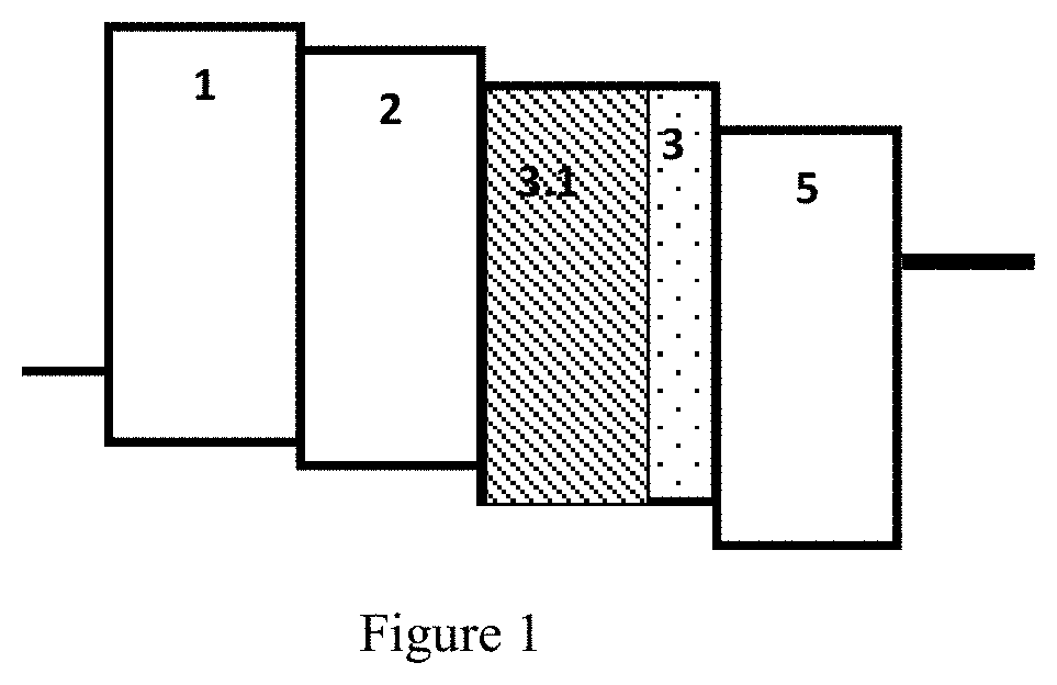
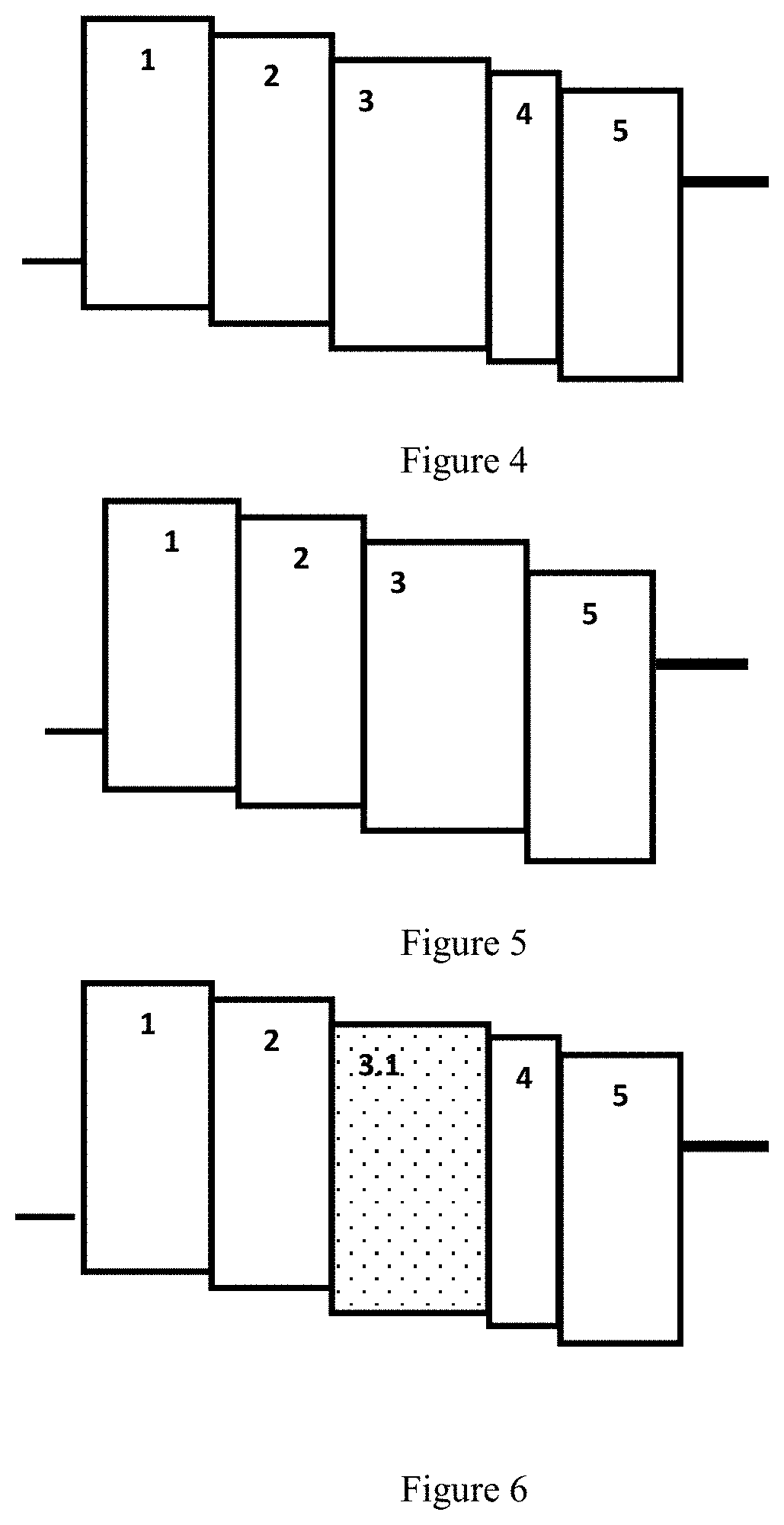
[0150]The structure of the OLED device of this Example is as shown in FIG. 1, and comprises: an anode, a hole injection layer 1, a hole transport layer 2, a luminescent layer 3, a barrier layer 4, an electron transport layer 5 and a cathode (not shown in the figure) that are successively laminated and deposited on a substrate (not shown in the figure).

[0151]In this Comparative Example, ITO serves as the anode; MTDATA:4% F4TCNQ serves as the hole injection layer 1; TCTA serves as the hole transport layer 2; the luminescent layer 3 employs the host (2-13) as the phosphorescence host material, and the green phosphorescence material Ir(ppy)3 serves as the green phosphorescence dye (the doping mass percentage of the dye in the luminescent layer is 1%); MTDATA doped Li3N serves as the electron transport layer 5; and Al serves as the cathode.

[0152]ITO / MTDATA:4% F4TCNQ(100 nm) / TCTA(20 nm) / host(2-13):1% Ir(ppy)3(30 nm) / Alq3:2% Li3N(25 nm) / Al(100 nm)

example 2

[0153]The structure of the OLED device of this Example is as shown in FIG. 1, and comprises: an anode, a hole injection layer 1, a hole transport layer 2, a luminescent layer 3, a barrier layer 4, an electron transport layer 5 and a cathode (not shown in the figure) that are successively laminated and deposited on a substrate (not shown in the figure).

[0154]In this Comparative Example, ITO serves as the anode; MTDATA:4% F4TCNQ serves as the hole injection layer 1; TCTA serves as the hole transport layer 2; the luminescent layer 3 employs the host (2-13) as the phosphorescence host material, and the green phosphorescence material Ir(ppy)3 serves as the green phosphorescence dye (the doping mass percentage of the dye in the luminescent layer is 5%); MTDATA doped Li3N serves as the electron transport layer 5; and Al serves as the cathode.

[0155]ITO / MTDATA:4% F4TCNQ(100 nm) / TCTA(20 nm) / host(2-13):5% Ir(ppy)3(30 nm) / Alq3:2% Li3N(25 nm) / Al(100 nm)

example 3

[0156]The structure of the OLED device of this Example is as shown in FIG. 1, and comprises: an anode, a hole injection layer 1, a hole transport layer 2, a luminescent layer 3, a barrier layer 4, an electron transport layer 5 and a cathode (not shown in the figure) that are successively laminated and deposited on a substrate (not shown in the figure).

[0157]In this Comparative Example, ITO serves as the anode; MTDATA:4% F4TCNQ serves as the hole injection layer 1; TCTA serves as the hole transport layer 2; the luminescent layer 3 employs the host (2-13) as the phosphorescence host material, and the green phosphorescence material Ir(ppy)3 serves as the green phosphorescence dye (the doping mass percentage of the dye in the luminescent layer is 10%); MTDATA doped Li3N serves as the electron transport layer 5; and Al serves as the cathode.

[0158]ITO / MTDATA:4% F4TCNQ(100 nm) / TCTA(20 nm) / host(2-13):10% Ir(ppy)3(3 On m) / Alq3:2% Li3N(25 nm) / Al(100 nm)


PUM

PropertyMeasurementUnit
singlet state energyaaaaaaaaaa
external quantum efficiencyaaaaaaaaaa

Abstract

The present invention discloses an organic electroluminescence device, comprising a luminescent layer, wherein, a host material of the luminescent layer comprises a thermally activated delayed fluorescence material, the host material is doped by a dye, and the dye comprises at least one phosphorescent dye. The present invention employs a thermally activated delayed fluorescence material, whose difference between the triplet state energy level and the singlet state energy level (ΔEST) is relatively small. The present invention employs the material as the phosphorescence host, so part of the triplet state exciton level transfers to the singlet state excitons, and the amount of the overall triplet state excitons is smaller. Therefore, the concentration of the triplet state excitons decreases, and the recombination region becomes narrower, which effectively reduces the probability of excitons entering the charge transport layer, and at the same time the narrowing of the recombination region effective prevents the diffusion of N-type dopants into the exciton recombination region. Additionally, by employing the host material, the device corresponds to a low working voltage.

Description

TECHNICAL FIELD[0001]The present invention relates to the field of organic electroluminescence device, and particularly to an organic electroluminescence device whose luminescent layer employs a novel host material.BACKGROUND OF THE PRESENT INVENTION[0002]Organic electroluminescence devices have drawn the broad attention of people due to the advantages such as thin bodies, large planar sizes, complete fixation and good flexibility, and organic white electroluminescence devices have become a research hotspot because of the great potential in solid state illumination light source and liquid crystal backlight light source.[0003]As early as in 1950s, Bernanose. A et al began the research on organic electroluminescence devices (OLED). The initial research material was anthracene single crystal wafer. Because of the problem of the large thickness of the single crystal wafer, the required driving voltage was very high. In 1987, C. W. Tang and Vanslyke of Eastman Kodak Company of the USA re...

Claims


Application Information

Patent Timeline
Patent Type & Authority Patents(United States)
IPC IPC(8): H01L51/00H01L51/52H01L51/50C09K11/06
CPCH01L51/0072C09K11/06H01L51/0067H01L51/0085C09K2211/1018H01L51/5221H01L51/5206C09K2211/1029H01L51/0097H01L51/5056H01L51/5016C09K2211/185H01L51/5088H01L2251/5338H01L51/5072H10K50/121H10K50/11H10K2101/40H10K2101/10H10K50/00H10K2101/20H10K85/626H10K85/633H10K85/6572H10K85/654H10K85/342H10K50/15H10K50/16H10K50/17H10K50/81H10K50/82H10K77/111H10K2102/311
Inventor DUAN, LIANQIU, YONGZHANG, GUOHUILI, MANZHANG, DONGDONGHU, YONGLAN
Owner BEIJING VISIONOX TECH
Why Eureka
Try Eureka