
Method for curing an overcoat in a photoconductor used in an electrophotographic imaging device

a photoconductor and photoconductor technology, applied in the field of methods, can solve the problems of mechanical abrasion of the surface layer of the photoconductor drum, easy scratches and abrasions, and the use of organic photoconductor drums

Active Publication Date: 2020-04-14
LEXMARK INT INC
View PDF6 Cites 0 Cited by
  • Summary
  • Abstract
  • Description
  • Claims
  • Application Information

AI Technical Summary

Benefits of technology

The method significantly increases the edge-wear resistance of the photoconductor drum, extending its lifespan and maintaining image quality, allowing it to print up to 150,000 pages without replacement, compared to the typical 5,000 to 50,000 pages, thus reducing costs and waste.

Problems solved by technology

Conversely, the surface of an organic photoconductor drums is typically comprised of a low molecular weight charge transport material, and an inert polymeric binder and are susceptible to scratches and abrasions.
Therefore, the drawback of using organic photoconductor drums typically arises from mechanical abrasion of the surface layer of the photoconductor drum due to repeated use.
Abrasion of photoconductor drum surface may arise from its interaction with print media (e.g. paper), paper dust, or other components of the electrophotographic image forming device such as the cleaner blade or charge roll.
The abrasion of photoconductor drum surface degrades its electrical properties, such as sensitivity and charging properties.
Electrical degradation results in poor image quality, such as lower optical density, and background fouling.
When a photoconductor drum is locally abraded, images often have black toner bands due to the inability to hold charge in the thinner regions.
This black banding on the print media often marks the end of the life of the photoconductor drum, thereby causing the owner of the printer with no choice but to purchase another expensive photoconductor drum or a new image unit, or in some cases, the whole cartridge altogether.
However, this overcoat layer does not lead to the robustness needed for edge wear in organic photoconductor drums used in direct-to-paper printing.
While the use of these urethane acrylate overcoat formulations have reduced the drum wear overall in an organic photoconductor, the improvement in paper edge wear resistance in the organic photoconductor drum in direct-to-paper printing has not been realized.

Method used


Image

  • Method for curing an overcoat in a photoconductor used in an electrophotographic imaging device
  • Method for curing an overcoat in a photoconductor used in an electrophotographic imaging device
  • Method for curing an overcoat in a photoconductor used in an electrophotographic imaging device

Examples


Embodiment Construction

[0014]It is to be understood that the disclosure is not limited in its application to the details of construction and the arrangement of components set forth in the following description or illustrated in the drawings. The disclosure is capable of other embodiments and of being practiced or of being carried out in various ways. Also, it is to be understood that the phraseology and terminology used herein is for the purpose of description and should not be regarded as limiting. The use of “including,”“comprising,” or “having” and variations thereof herein is meant to encompass the items listed thereafter and equivalents thereof as well as additional items. Further, the terms “a” and “an” herein do not denote a limitation of quantity, but rather denote the presence of at least one of the referenced item.

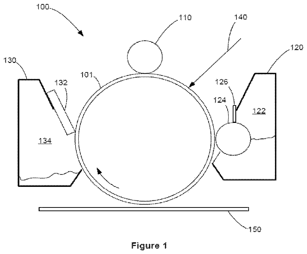
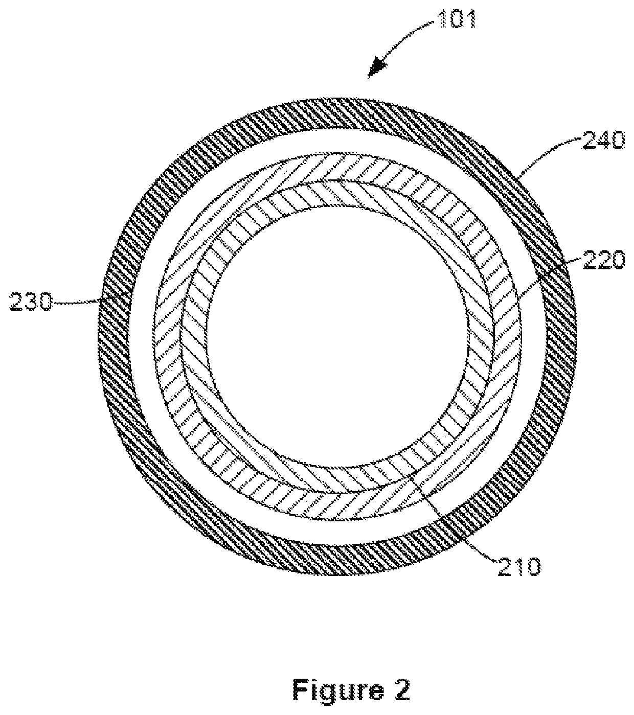
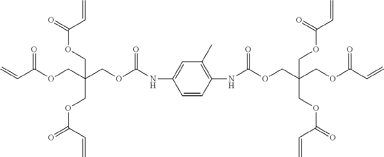
[0015]FIG. 1 illustrates a schematic representation of an example electrophotographic image forming device 100. Image forming device 100 includes a photoconductor drum 101, a charge ro...


PUM

PropertyMeasurementUnit
diameteraaaaaaaaaa
timeaaaaaaaaaa
currentaaaaaaaaaa

Abstract

A method of curing a protective overcoat layer on the outermost portion of an organic photoconductor drum using dual curing process is provided. The first curing step applies either ionizing irradiation, such as with an electron beam or by gamma rays or applies non-ionizing irradiation such as ultraviolet light to the overcoated photoconductor drum. A mask or shield is sized to be placed over the print area of the initially cured photoconductor drum, thereby exposing the outermost edges of the photoconductor drum. The outer edges of the masked photoconductor drum is then exposed to a second curing step using non-ionizing irradiation such as ultraviolet light.

Description

CROSS REFERENCES TO RELATED APPLICATIONS[0001]This patent application is a continuation application of U.S. patent application Ser. No. 16 / 225,337, filed Dec. 19, 2018, entitled “Method for Curing an Overcoat in a Photoconductor Used in an Electrophotographic Imaging Device”, which is a continuation application of U.S. patent application Ser. No. 15 / 845,201, filed Dec. 18, 2017, entitled “Method for Curing an Overcoat in a Photoconductor Used in an Electrophotographic Imaging Device”.BACKGROUND[0002]1.Field of the Disclosure[0003]The present disclosure relates generally to electrophotographic image forming devices, and more particularly to a method of curing an overcoat layer placed on the outermost surface of an organic photoconductor drum used in an electrophotographic image forming device. The disclosed method of curing the overcoat is a two-step process. The first curing step applies either ionizing irradiation, such as with an electron beam (‘EB’) or by gamma rays or applies no...

Claims


Application Information

Patent Timeline
Patent Type & Authority Patents(United States)
IPC IPC(8): G03G7/00G03G5/05G03G5/147
CPCG03G5/0525G03G5/147G03G7/0006G03G5/14791
Inventor LUO, WEIMEIBELLINO, MARK THOMASHROBSKY, RUDOLPH WAYNE
Owner LEXMARK INT INC
Learn More