Laser diode device

a laser diode and diode technology, applied in the direction of laser details, semiconductor lasers, electrical apparatus, etc., can solve the problems of laser diode driving speed reduction, driving signal strength reduction, so as to reduce the driving speed of laser diode, the effect of reducing the strength of the driving signal and losing the strength

Active Publication Date: 2020-07-07
SHANGHAI ORIENT CHIP TECH CO LTD
View PDF11 Cites 0 Cited by
  • Summary
  • Abstract
  • Description
  • Claims
  • Application Information

AI Technical Summary

Benefits of technology

[0003]The longer the route taken to transmit a driving signal is, the more the driving signal loses its strength because of the electrical properties, such as impedance, of the route. The reduction in the strength of the driving signal leads to a reduction in the laser diode driving speed, to the detriment of recognition speed and efficiency. To increase the laser diode driving speed by reducing the signal transmission distance between the laser diode and a driving chip, the present invention provides a laser diode device which comprises a laser diode component, a lens, a first carrying element, a driving chip, a second carrying element, a laser diode module and a driving chip module. The first carrying element receives the laser diode component and the lens. The second carrying element receives the driving chip and is disposed below the first carrying element to carry the first carrying element and is electrically connected to the first carrying element.

Problems solved by technology

The longer the route taken to transmit a driving signal is, the more the driving signal loses its strength because of the electrical properties, such as impedance, of the route.
The reduction in the strength of the driving signal leads to a reduction in the laser diode driving speed, to the detriment of recognition speed and efficiency.
Furthermore, with two carrying elements being adapted to achieve thermal and electrical separation of the laser diode component and the driving chip, the performance of the driving chip remains unabated despite the heat generated by the laser diode component in operation.

Method used


Image

  • Laser diode device
  • Laser diode device

Examples


Embodiment Construction

[0017]To facilitate understanding of the object, characteristics and effects of this present disclosure, embodiments together with the attached drawings for the detailed description of the present disclosure are provided.

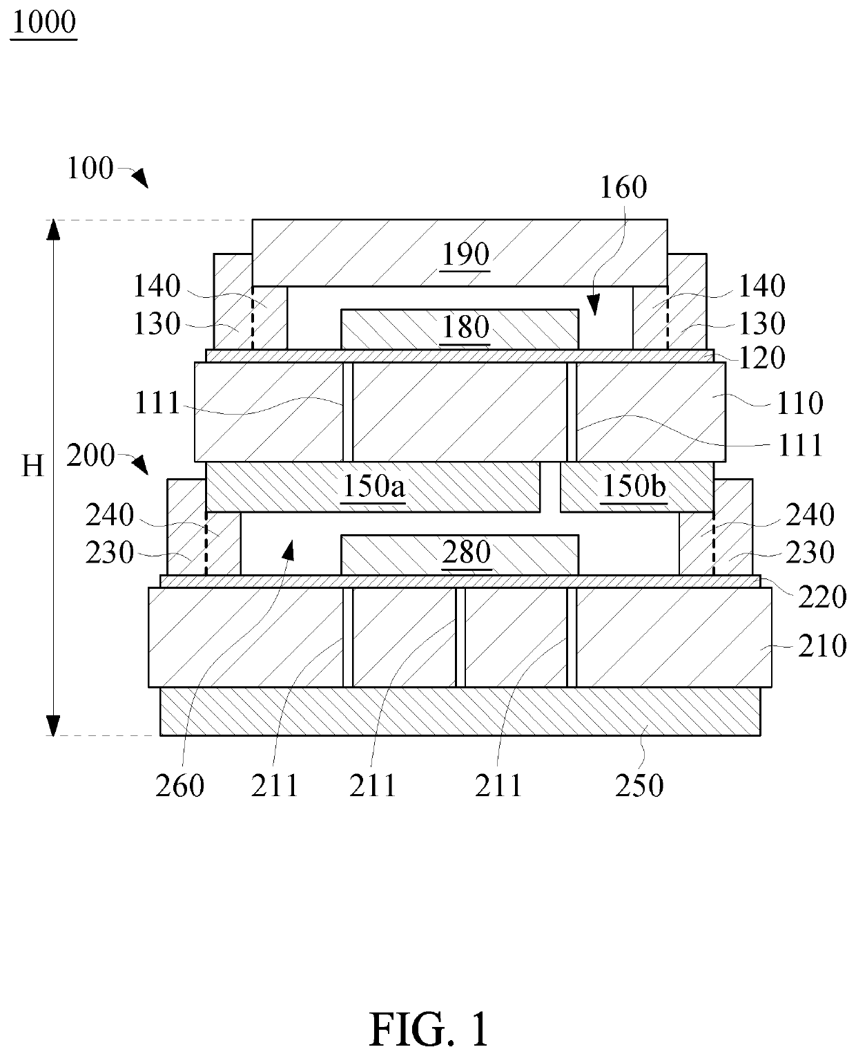
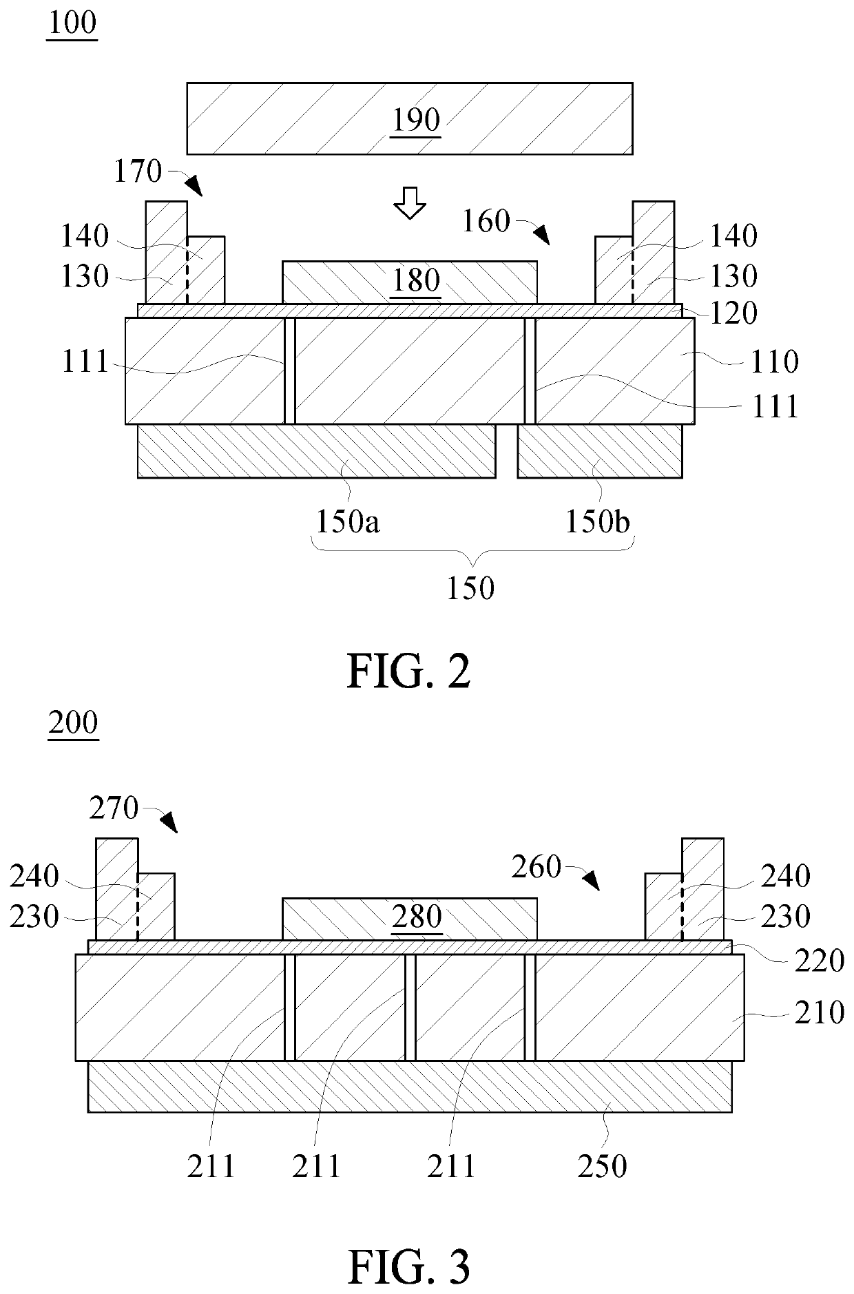
[0018]FIG. 1 is a schematic view of a package structure of a laser diode device 1000 according to an embodiment of the present disclosure. The laser diode device 1000 comprises a laser diode module 100 and a driving chip module 200. FIG. 2 is a schematic view of the standalone structure of the laser diode module 100 according to an embodiment of the present disclosure. FIG. 3 is a schematic view of a standalone structure of the driving chip module 200 according to an embodiment of the present disclosure.

[0019]The laser diode module 100 comprises a first carrying element. The first carrying element receives and carries a laser diode component 180 (such as a laser diode chip) and a lens 190. The first carrying element comprises a first ceramic carrier 110, a first met...


PUM

PropertyMeasurementUnit
heightaaaaaaaaaa
transmission distanceaaaaaaaaaa
timeaaaaaaaaaa

Abstract

A laser diode device includes a laser diode component, a lens, a first carrying element, a driving chip and a second carrying element. The first carrying element receives the laser diode component and the lens. The second carrying element receives the driving chip and is disposed below the first carrying element to carry the first carrying element and electrically connected to the first carrying element.

Description

BACKGROUND OF THE INVENTION1. Field of the Invention[0001]The present disclosure relates to laser diode devices, and in particular to a laser diode device capable of reducing a signal transmission distance.2. Description of the Related Art[0002]Thanks to their advantages, better linearity, micro-spots and high laser density, laser diodes are widely used in reading, communication, measurement, sensing, etc. In recent years, laser diodes are widely applicable to facial recognition and object recognition provided by mobile devices (such as smartphones and tablets), for example, to perform facial recognition in conjunction with time of flight (ToF) technology. A conventional laser diode often operates in conjunction with a driving signal generated by a driving chip and thereby emits laser according to the driving signal received. Hence, the control over the driving speed of the laser diode depends on the driving signal received. Recognition efficiency depends directly on the driving spe...

Claims


Application Information

Patent Timeline
Patent Type & Authority Patents(United States)
IPC IPC(8): H01S5/02H01S5/022H01S5/042H01S5/026H01S5/02315
CPCH01S5/02252H01S5/0206H01S5/02288H01S5/0425H01S5/0261H01S5/04257H01S5/042H01S5/06226H01S5/183H01S5/023H01S5/0233H01S5/0235H01S5/02257H01S5/02345H01S5/02315H01S5/02326H01S5/02253
Inventor LUO, JIEHUANG, LIEN-CHUANWU, CHI-MING
Owner SHANGHAI ORIENT CHIP TECH CO LTD
Why Eureka
Try Eureka