Supercharge Your Innovation With Domain-Expert AI Agents!

Naturally closed MEMs switch for ESD protection

a technology of esd protection and mems switch, which is applied in the direction of semiconductor devices, contact details, semiconductor/solid-state devices, etc., can solve the problems of significant performance penalty when applied to radio-frequency components, and degrade such performance to unacceptable levels

Active Publication Date: 2021-03-30
QORVO US INC
View PDF17 Cites 4 Cited by
  • Summary
  • Abstract
  • Description
  • Claims
  • Application Information

AI Technical Summary

Benefits of technology

[0006]In one embodiment, a MEMS device comprises a substrate having a first anchor electrode and an RF electrode disposed therein; a switching element comprising a stress layer, a bottom layer and a top layer, wherein the bottom layer is coupled to the top layer at a first end and the bottom layer is coupled to the anchor electrode at the second end and wherein the stress layer is under tensile stress.

Problems solved by technology

These solutions come with a significant performance penalty when applied to radio-frequency components.
But traditional ESD protection techniques would degrade such performance to unacceptable levels.

Method used


Image

  • Naturally closed MEMs switch for ESD protection
  • Naturally closed MEMs switch for ESD protection
  • Naturally closed MEMs switch for ESD protection

Examples


Embodiment Construction

[0016]The present disclosure generally relates to a MEMS device for reducing ESD. A contacting switch is used to ensure that there is a closed electrical contact between two electrodes even if there is no applied bias voltage.

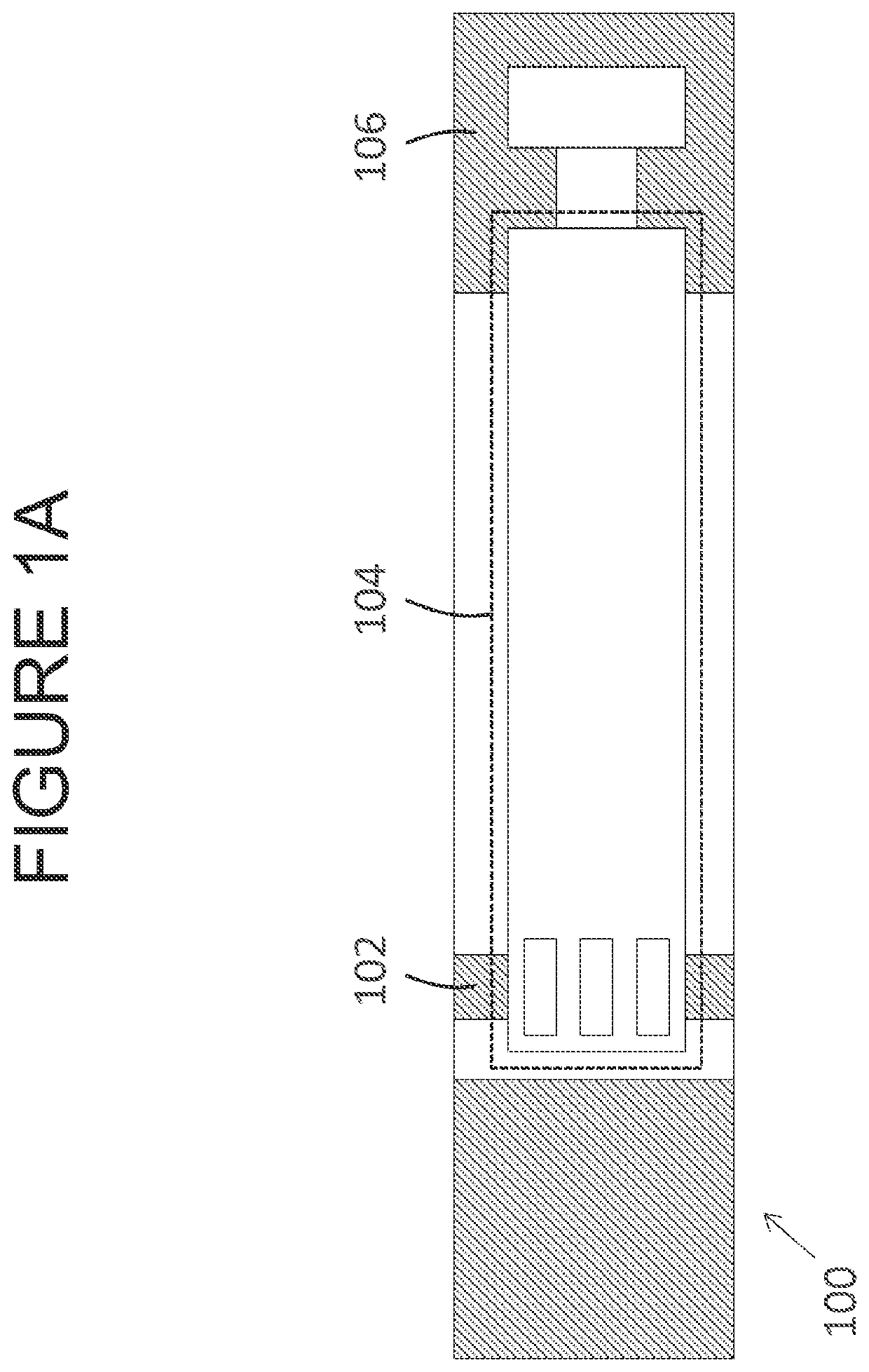
[0017]FIG. 1A is a schematic top-view of a naturally closed ohmic MEMS switch 100. The switch 100 contains an RF-electrode 102, control-electrode 104 and anchor electrode 106. The switch provides for an ohmic contact between 102 and 106 in the unpowered state. The contact between 102 and 106 can be broken by applying a high-enough voltage to the control-electrode 106.

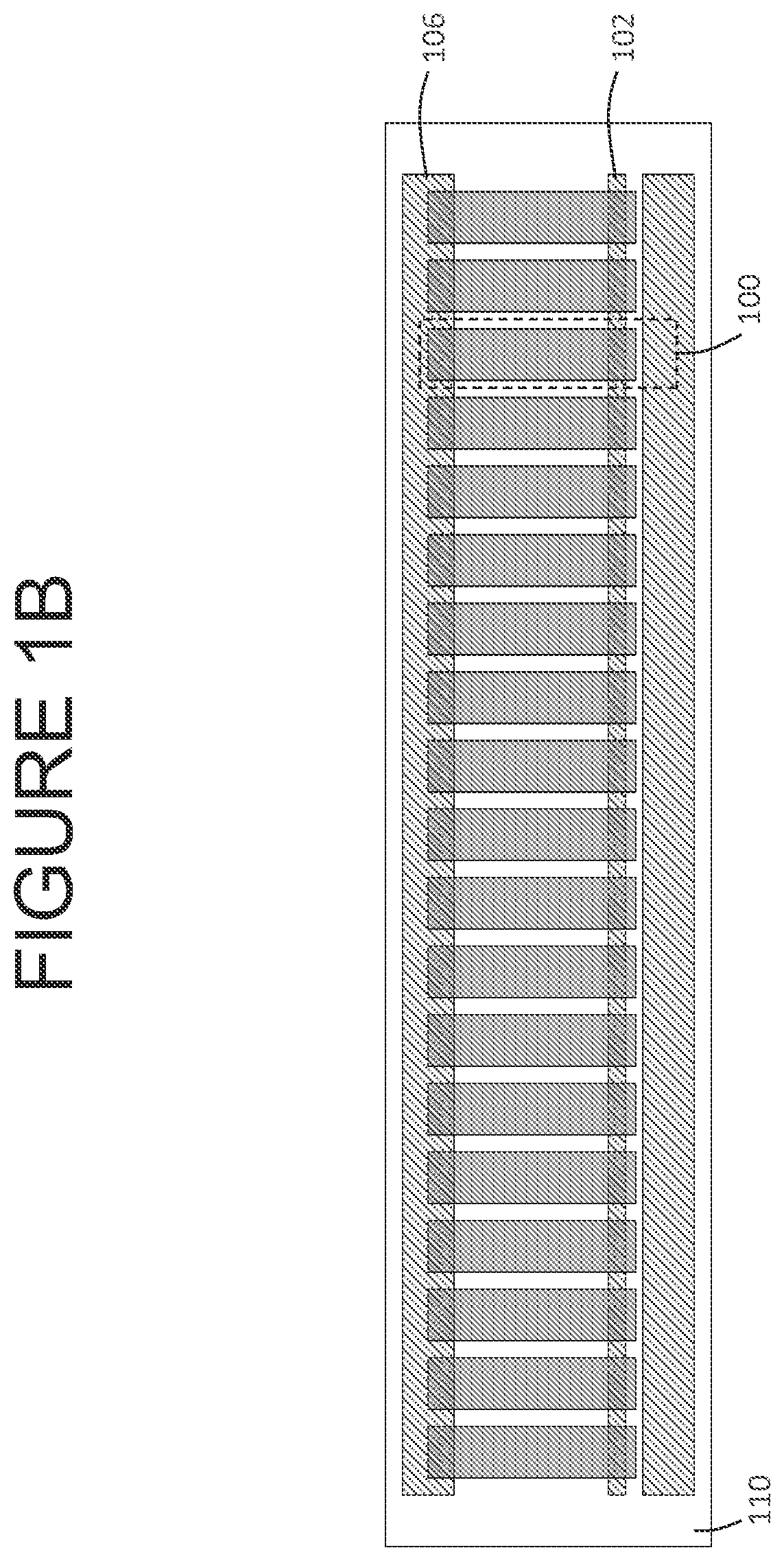
[0018]FIG. 1B is a schematic top view of a naturally closed ohmic MEMS switch cell 110 containing a number of naturally closed MEMS switches 100. All MEMS switches 100 in the cell 110 are operated in parallel and collectively have a lower resistance between the electrodes 102 and 106. All switches can be turned off by applying a high-enough voltage to the control-electrode.

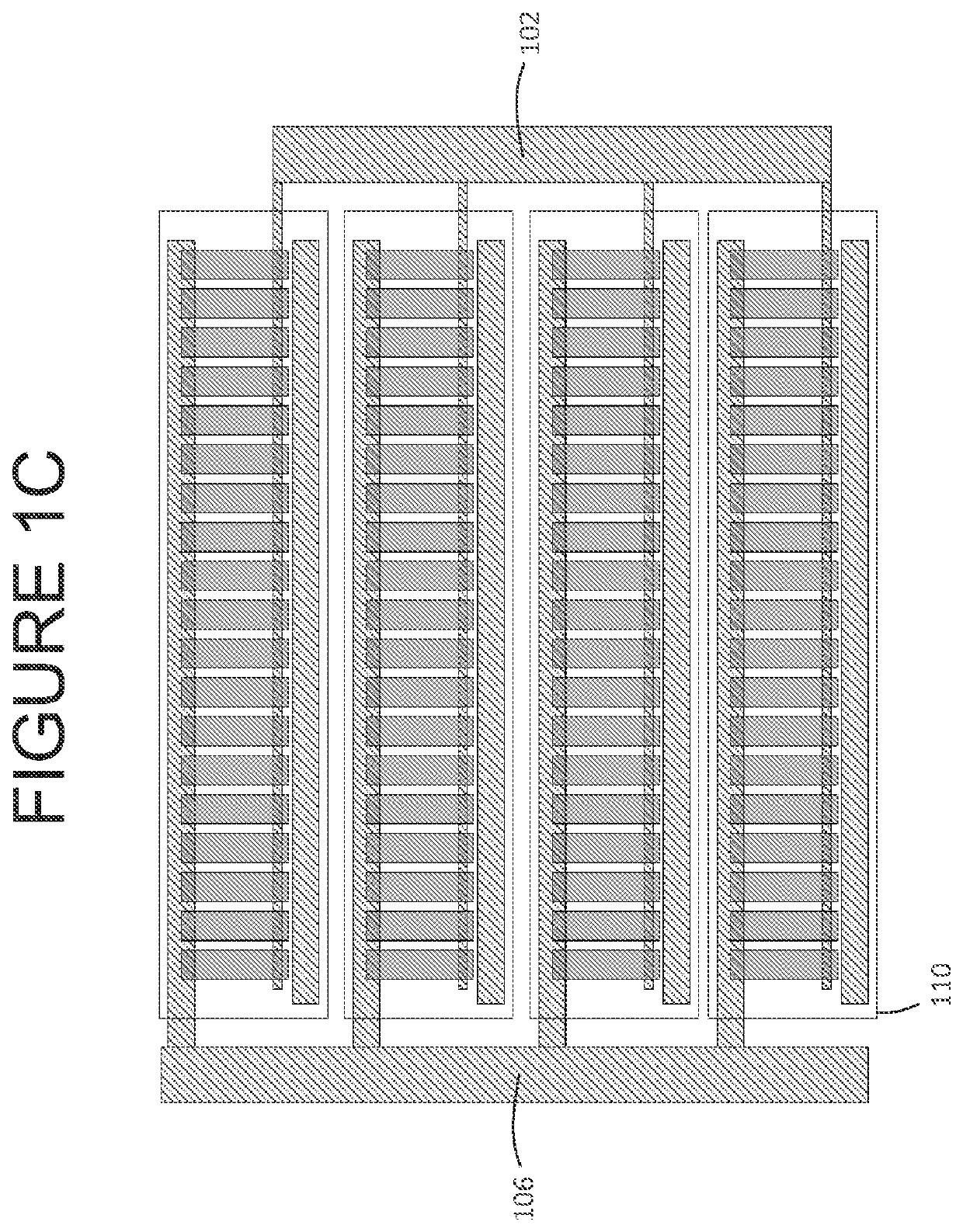
[0019]FIG. 1C shows a sch...


PUM

PropertyMeasurementUnit
control voltageaaaaaaaaaa
thicknessaaaaaaaaaa
tensile stressaaaaaaaaaa

Abstract

The present disclosure generally relates to a MEMS device for reducing ESD. A contacting switch is used to ensure that there is a closed electrical contact between two electrodes even if there is no applied bias voltage.

Description

BACKGROUND OF THE DISCLOSUREField of the Disclosure[0001]Embodiments of the present disclosure generally relate to a micro electromechanical systems (MEMS) device for reducing risk of electro-static discharge (ESD).Description of the Related Art[0002]Devices including MEMS technology which have been designed and manufactured for applications in radio frequency telecommunications where risk of electro-static discharge is present, both during the manufacturing process (e.g. assembly) and in the typical usage conditions of the device (e.g. exposure to electrically charged human body). In particular, components such switches and tunable capacitors used to enable reconfigurable analog and mixed-signal circuits for state-of-the-art wireless devices.[0003]ESD protection devices and circuits are an essential part of the solid state technology enabling electronic components and circuits. These solutions come with a significant performance penalty when applied to radio-frequency components. K...

Claims


Application Information

Patent Timeline
Patent Type & Authority Patents(United States)
IPC IPC(8): H01H59/00H01L23/60H01H1/00
CPCH01H59/0009H01L23/60H01H2001/0078
Inventor VAN KAMPEN, ROBERTUS PETRUSBARRON, LANCEGADDI, ROBERTOKNIPE, RICHARD L.
Owner QORVO US INC
Features
  • R&D
  • Intellectual Property
  • Life Sciences
  • Materials
  • Tech Scout
  • Unparalleled Data Quality
  • Higher Quality Content
  • 60% Fewer Hallucinations
Learn More