Semiconductor device having plug and metal line

a technology of electromagnetic field and metal line, applied in the direction of electromagnetic field, basic electric elements, electrical apparatus, etc., can solve the problem of reducing the size of features

Active Publication Date: 2021-06-15
UNITED MICROELECTRONICS CORP +1
View PDF3 Cites 0 Cited by
  • Summary
  • Abstract
  • Description
  • Claims
  • Application Information

AI Technical Summary

Benefits of technology

[0004]It is one of the primary objectives of the present invention to provide a semiconductor device and a method of forming the same, in which a multiple patterning process such as a self-aligned double patterning (SADP) process is utilized to form tiny structures with different pitches, dimensions and shapes in different regions according to the requirements of practical products. That is, a smaller, more densely packed semiconductor structure may be formed under a simplified process flow by using a reduced number of photomasks, to provide particular layout due to various requirements of semiconductor products.
[0007]In summary, the forming method of the present invention utilizes a multiple patterning process such as a self-aligned double patterning (SADP) process to form tiny structures within various regions of the semiconductor device. The forming method for example carries out two SADP processes in one region to form target patterns in array arrangement and finer, more densely layout, corresponding to conductive structures underneath. While performing the two SADP processes, other target patterns with different pitches, dimensions and shapes is formed in another region, with those target patterns with different pitches, dimensions and shapes being not corresponding to the conductive structures underneath. That is, the forming method of the present invention not only can form target patterns with different pitches, dimensions, shapes, and arrangements indifferent regions via the same forming processes, but also makes the target patterns formed within the same region to further obtain various pitches, dimensions and shapes, so as to meet the practical requirements of products. In this way, the forming method of the present invention enables to form the semiconductor device having particular layouts in particular regions, under a simplified process.

Problems solved by technology

As feature sizes are decreased by the complexity of currently integrated circuits, the existing single patterning process has met its bottleneck to successfully render the features.
That is, the overlay accuracy and the resolution among this feature have to push the lithographic limit further to create even smaller, more densely packed devices.

Method used


Image

  • Semiconductor device having plug and metal line
  • Semiconductor device having plug and metal line
  • Semiconductor device having plug and metal line

Examples


Embodiment Construction

[0027]To provide a better understanding of the presented invention, preferred embodiments will be described in detail. The preferred embodiments of the present invention are illustrated in the accompanying drawings with numbered elements.

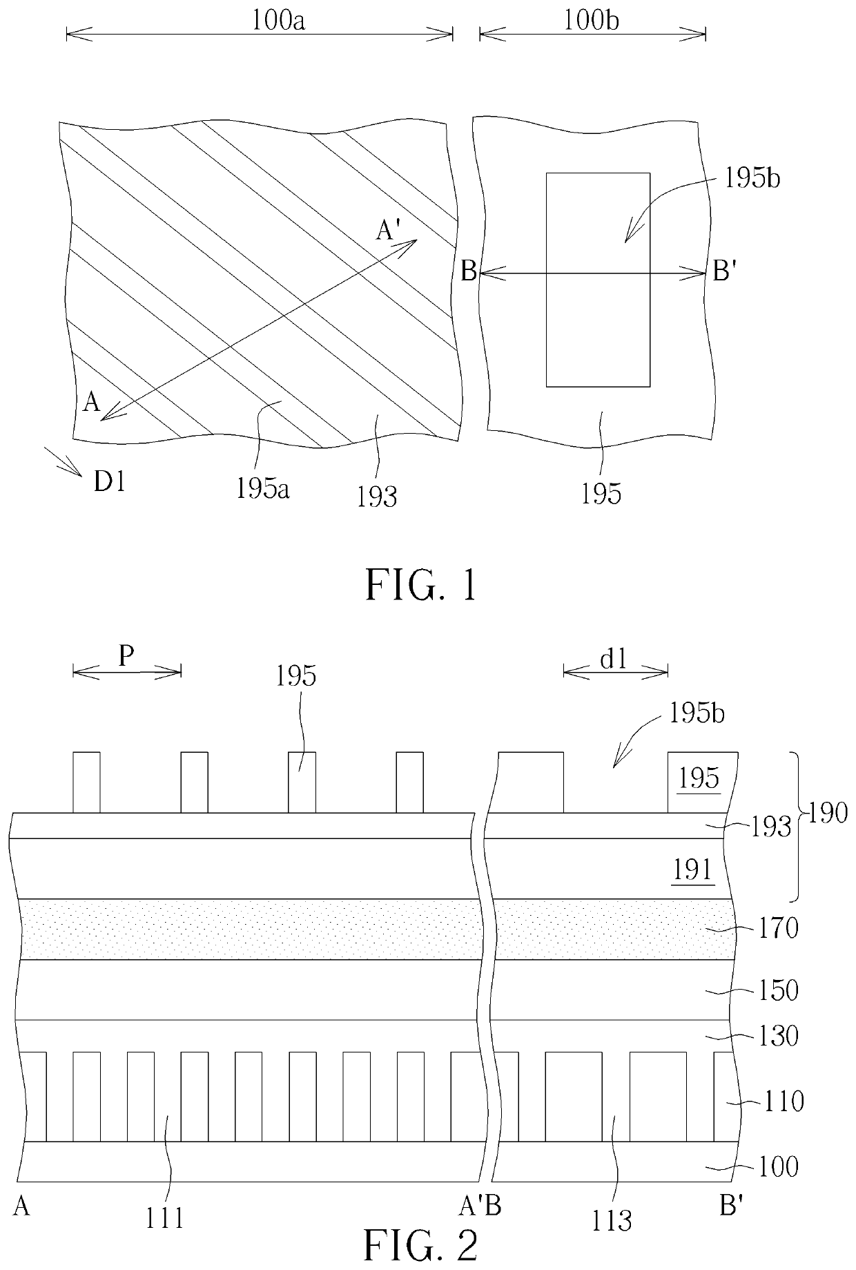
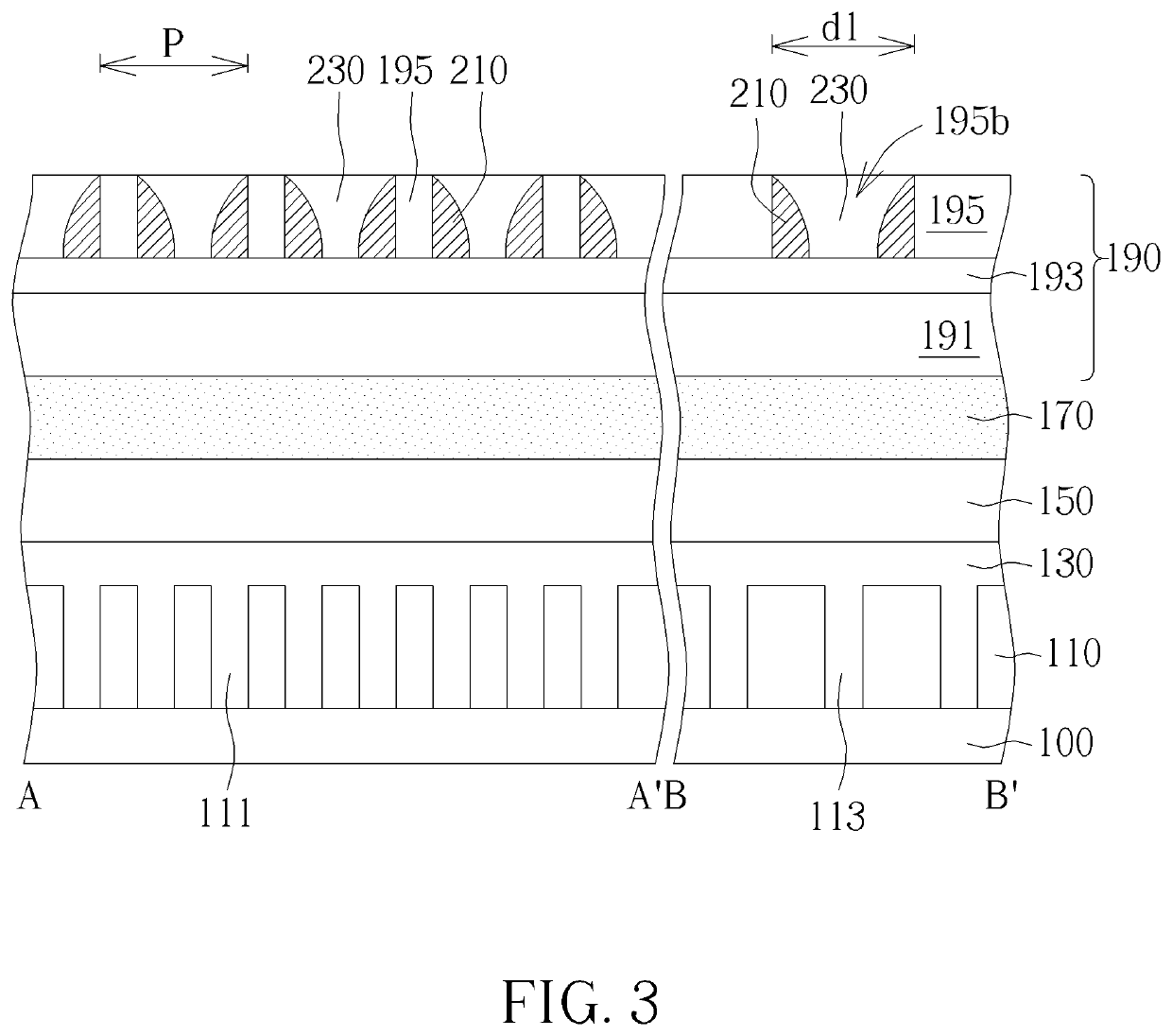
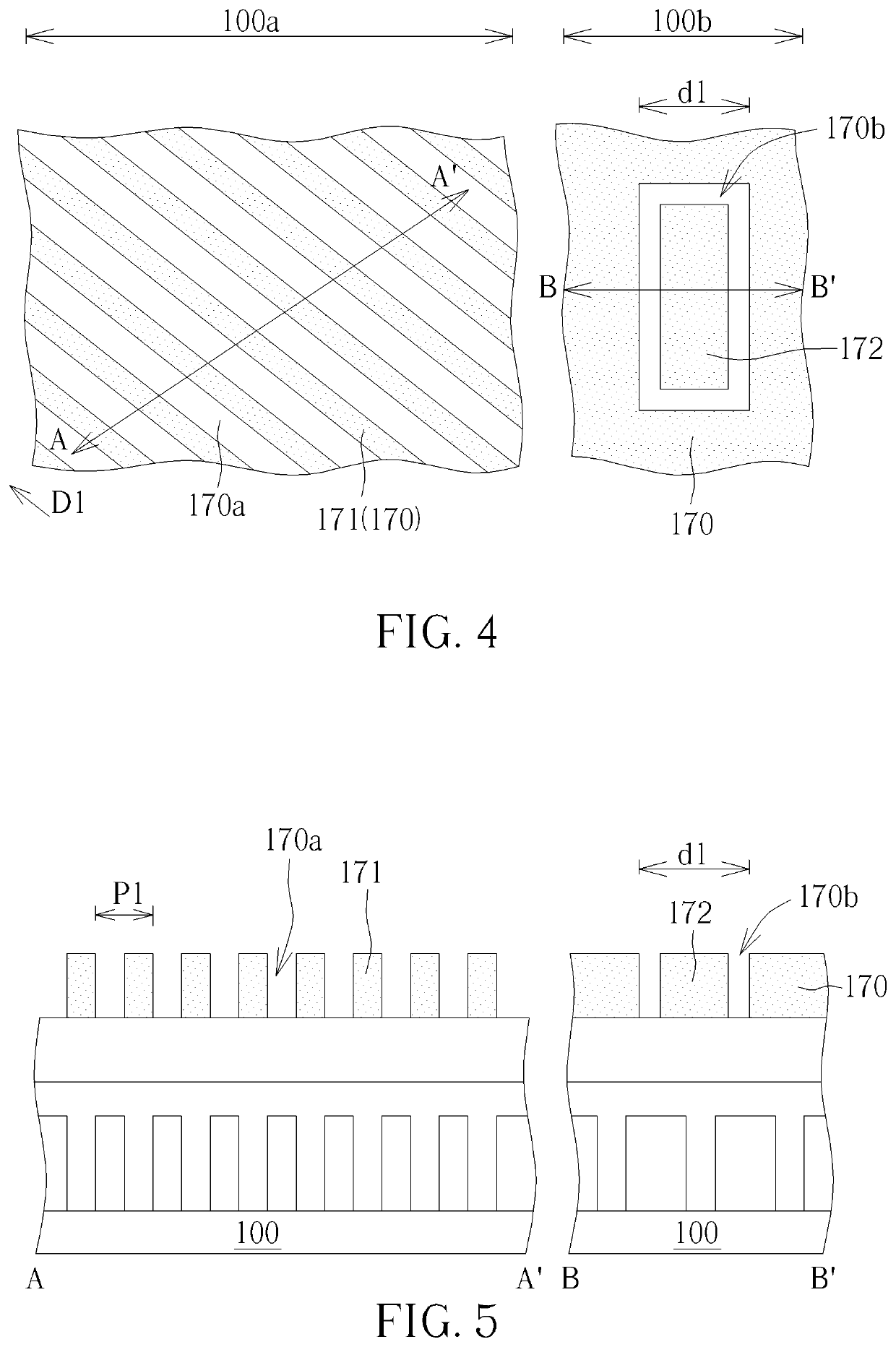
[0028]Please refer to FIG. 1 to FIG. 12, which are schematic diagrams illustrating a forming process of a semiconductor device according to the preferred embodiment of the present invention, wherein FIGS. 1, 4, 6, 7, 8 and 10 respectively show a top view of a semiconductor device during the forming process, and other figures respectively show a cross-sectional view taken along cross lines A-A′ and B-B′ in FIGS. 1, 4, 6, 7, 8 and 10.

[0029]First of all, a substrate 100 is provided, for example a semiconductor substrate like a silicon substrate, a silicon containing substrate, an epitaxial silicon substrate or a silicon-on-insulator (SOI) substrate, and a first region 100a such as a core region of the semiconductor device, and a second region 100b such...


PUM

PropertyMeasurementUnit
cross angleaaaaaaaaaa
distanceaaaaaaaaaa
areaaaaaaaaaaa

Abstract

A semiconductor device and a method of forming the same, the semiconductor device includes a substrate, a gate structure, a first dielectric layer, a second dielectric layer, a first plug and two metal lines. The substrate has a shallow trench isolation and an active area, and the gate structure is disposed on the substrate to cover a boundary between the active area and the shallow trench isolation. The first dielectric layer is disposed on the substrate, to cover the gate structure, and the first plug is disposed in the first dielectric layer to directly in contact with a conductive layer of the gate structure and the active area. The second dielectric layer is disposed on the first dielectric layer, with the first plug and the gate being entirely covered by the first dielectric layer and the second dielectric layer. The two metal lines are disposed in the second dielectric layer.

Description

BACKGROUND OF THE INVENTION1. Field of the Invention[0001]The present invention relates to a semiconductor device and a method of forming a semiconductor device, and more particularly to a semiconductor device being formed through a multiple patterning process and a method of forming the same.2. Description of the Prior Art[0002]Fabrication of microstructures requires tiny elements of precisely controlled size formed in a material layer of an appropriate substrate such as semiconductor substrate / layers, dielectric layers and / or metal layers. These tiny elements are generated by patterning the abovementioned substrate / layers, for instance, by performing photolithography and etching processes. For this purpose, in conventional semiconductor techniques, a mask layer is formed on the target, and these tiny elements are defined in the mask layer and followed by being transferred to the target layer. Generally, the mask layer may include or is formed by means of a layer of photoresist tha...

Claims


Application Information

Patent Timeline
Patent Type & Authority Patents(United States)
IPC IPC(8): H01L29/76H01L29/06H01L21/027H01L29/66H01L21/3213H01L21/033H01L21/311
CPCH01L29/0649H01L21/0274H01L21/0337H01L21/0338H01L21/31111H01L21/32133H01L21/32139H01L29/66545H01L29/66795H01L21/76816H01L29/78H01L29/4966H01L21/84H01L27/1203H10B12/09H10B12/50H10B12/0335
Inventor CHANG, FENG-YILEE, FU-CHECHANG, YI-CHINGHUANG, KAI-LOULIN, YING-CHIHLIN, GANG-YI
Owner UNITED MICROELECTRONICS CORP
Why Eureka
Try Eureka