
Flexible display

a flexible display and display panel technology, applied in non-linear optics, instruments, organic semiconductor devices, etc., can solve the problems of easy breakage of parts of film layers, failure of flexible display panels, etc., and achieve good bending tolerance

Active Publication Date: 2021-06-29
AU OPTRONICS CORP
View PDF12 Cites 0 Cited by
  • Summary
  • Abstract
  • Description
  • Claims
  • Application Information

AI Technical Summary

Benefits of technology

The design enhances the bending tolerance of flexible displays by distributing stress away from the film layers and ensuring the electrical performance of pixel structures when the display is bent.

Problems solved by technology

However, when the flexible display panel is bent, part of the film layers are easily broken due to poor stress tolerance, which in turn leads to failure of the flexible display panel.

Method used


Image

  • Flexible display
  • Flexible display
  • Flexible display

Examples


first embodiment

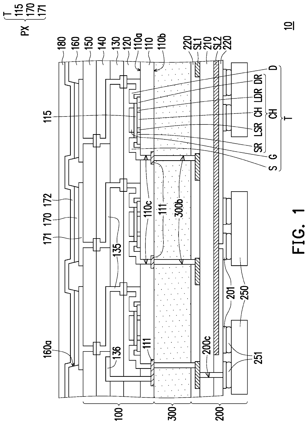
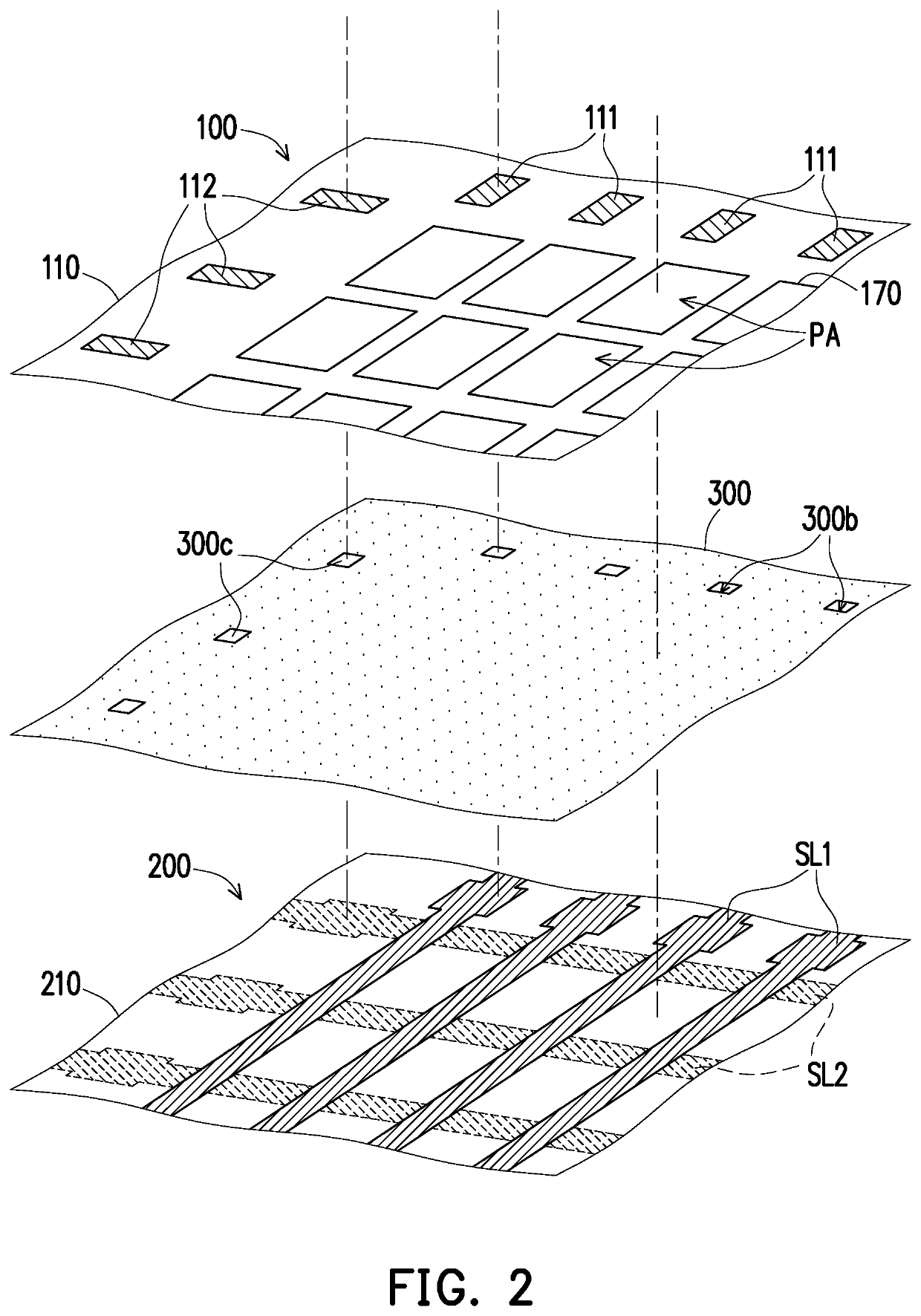
[0032]FIG. 1 is a schematic cross-sectional view of a flexible display according to the disclosure. FIG. 2 is a schematic top view of the flexible circuit board, the adhesive layer, and the pixel circuit layer of FIG. 1. It should be noted that, for a clear presentation, the flexible circuit board 200 of FIG. 2 omits the illustration of the protective layer 220, the fourth conductive through holes 200c, the conductors 251 and the driving chips 250 of FIG. 1, and the pixel circuit layer 100 of FIG. 2 only shows the buffer layer 110, the light emitting patterns 170, the first pads 111, and the second pads 112 of FIG. 1.

[0033]In the embodiment, a flexible display 10 may be a self-emitting display, and the self-emitting display includes, for example, an organic light emitting diode (OLED) display, a micro light emitting diode (micro-LED) display, or a mini light emitting diode (mini-LED) display. However, in other embodiments, the flexible display may also be a non-self-emitting display...

second embodiment

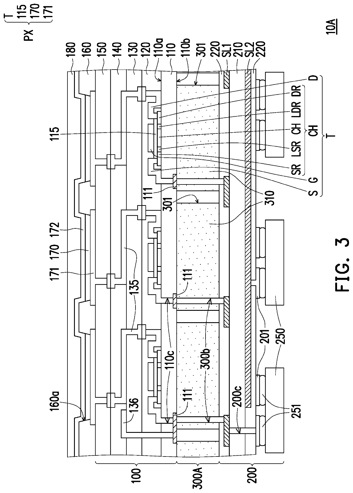
[0050]FIG. 3 is a schematic cross-sectional view of a flexible display according to the disclosure. FIG. 4 is a schematic top view of the flexible circuit board, the adhesive layer, and the pixel circuit layer of FIG. 3. It should be noted that, for a clear presentation, the flexible circuit board 200 of FIG. 4 omits the illustration of the protective layer 220, the fourth conductive through holes 200c, the conductors 251 and the driving chips 250 of FIG. 3, and the pixel circuit layer 100 of FIG. 4 only shows the buffer layer 110, the light emitting patterns 170, the first pads 111, and the second pads 112 of FIG. 3.

[0051]With reference to FIGS. 3 and 4, the difference between a flexible display 10A of this embodiment and the flexible display 10 of the previous embodiment lies in the structural design and disposition of an adhesive layer 300A of the flexible display 10A. Specifically, the adhesive layer 300A of the flexible display 10A has a plurality of first grooves 301, and an o...

third embodiment

[0053]FIG. 5 is a schematic cross-sectional view of a flexible display according to the disclosure. FIG. 6 is a schematic top view of the protective layer, the flexible circuit board, and the pixel circuit layer of FIG. 5. It should be noted that, for a clear presentation, the flexible circuit board 200 of FIG. 6 omits the illustration of the protective layer 220 of FIG. 5, and the pixel circuit layer 100 of FIG. 6 only shows the buffer layer 110, the light emitting patterns 170, the first pads 111, and the second pads 112 of FIG. 5.

[0054]With reference to FIGS. 5 and 6, the difference between a flexible display 10B of this embodiment and the flexible display 10 of the previous embodiment lies in that the flexible display 10B further includes a protective layer 190. In the embodiment, the protective layer 190 is disposed on a side of the flexible circuit board 200 away from the adhesive layer 300; that is, the flexible circuit board 200 is located between the adhesive layer 300 and ...


PUM

PropertyMeasurementUnit
crushing stressaaaaaaaaaa
anisotropic conductiveaaaaaaaaaa
conductiveaaaaaaaaaa

Abstract

A flexible display including a buffer layer, a plurality of pixel structures, a plurality of first pads, a plurality of first conductive through holes, a flexible circuit board and an adhesive layer is provided. The pixel structures are disposed on a first surface of the buffer layer. The first pads are disposed on a second surface of the buffer layer. The first conductive through holes are embedded in the buffer layer. The first pads are respectively electrically connected to the pixel structures through the first conductive through holes. The adhesive layer is disposed between the second surface of the buffer layer and the flexible circuit board. An orthogonal projection of the adhesive layer on the buffer layer overlaps an orthogonal projection of the pixel structures on the buffer layer. The first pads are electrically connected to first signal lines of the flexible circuit board.

Description

CROSS-REFERENCE TO RELATED APPLICATION[0001]This application claims the priority benefit of Taiwan application serial no. 108115697, filed on May 7, 2019. The entirety of the above-mentioned patent application is hereby incorporated by reference herein and made a part of this specification.BACKGROUNDTechnical Field[0002]The disclosure relates to a display, and more particularly to a flexible display.Description of Related Art[0003]With the development of display technology, the application range of display panels increasingly widens. For example, in the early days, the display panels were mostly used as the screens of electronic devices (such as televisions, computers, mobile phones, etc.), and the display panels applied to the electronic devices were mostly rigid display panels. Recently, some people have applied display panels to wearable devices (such as watches, clothes, etc.), and the display panels applied to the wearable devices are mostly flexible display panels.[0004]Flexib...

Claims


Application Information

Patent Timeline
Patent Type & Authority Patents(United States)
IPC IPC(8): H05K1/00H05K1/14H01L27/32H01L51/00H05K1/02H10K99/00
CPCH05K1/147H01L27/3276H01L51/0097H05K1/028H01L2251/5338H05K2201/10128H01L27/1218H01L27/1244H01L27/156G02F1/133305G02F1/13306G02F1/13452H10K59/131Y02E10/549H10K77/111H10K2102/311
Inventor HWU, KEH-LONGCHEN, YUNG-CHIHKE, TSUNG-YINGWANG, WAN-TSANGLIU, CHUN-HSIN
Owner AU OPTRONICS CORP
Learn More