
Method for joining a micorelectronic chip to a wire element

a technology of microelectronic chips and wire elements, which is applied in the direction of semiconductor devices, semiconductor/solid-state device details, textiles and paper, etc., can solve the problems of difficult to accurately position wires and reliably assemble them on the chip, and achieve the effect of precise and reliable fixing of wire elements on the chip

Active Publication Date: 2021-08-03
PRIMO1D
View PDF15 Cites 1 Cited by
  • Summary
  • Abstract
  • Description
  • Claims
  • Application Information

AI Technical Summary

Benefits of technology

This process relaxes the shape constraints of the chip, enabling precise and reliable fixation of the wire element without the need for specific groove formation on the chip, improving assembly efficiency and accuracy.

Problems solved by technology

The formation of grooves by assembly or engraving on the side faces of a chip is a delicate operation but also constraining in terms of the chip's structural configuration.
However, the absence of grooves on the chip makes it difficult to accurately position the wires and assemble them reliably on the chip, especially in an industrial context where it is necessary to maintain a high production rate.

Method used


Image

  • Method for joining a micorelectronic chip to a wire element
  • Method for joining a micorelectronic chip to a wire element
  • Method for joining a micorelectronic chip to a wire element

Examples


first embodiment

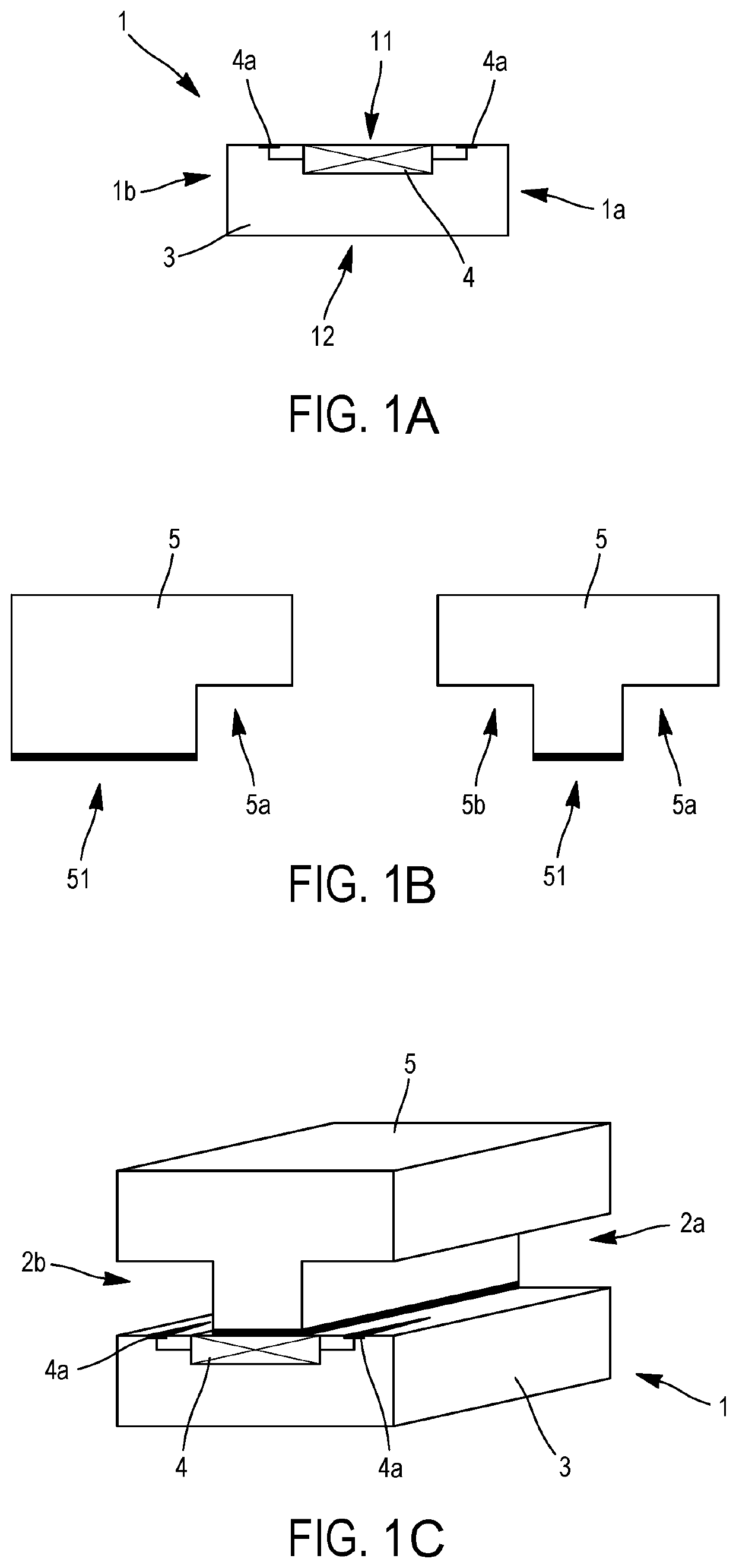
[0058] cover 5 has a contact face 51 intended to be applied to the first face 11 and having at least one shoulder 5a, 5b (FIG. 1B). This shoulder 5a, 5b makes it possible to form the temporary lateral groove 2a, 2b with the first side 11 of the microelectronic chip 1 when the cover 5 is applied to the chip 1 (FIG. 1C). According to this embodiment, the first side 11 is flat (or substantially flat after the manufacturing steps of the microelectronic component) and it is not necessary to create a specific groove. Advantageously, as shown in FIG. 1C, contact face 51 of cover 5, applied to the first face 11, has two shoulders 5a, 5b to form two parallel temporary lateral grooves 2a, 2b, with the first flat face 11 of the microelectronic chip 1.

[0059]Of course, the contact face 51 of cover 5 may have any number of shoulders, capable of forming temporary grooves, each arranged in any orientation, without departing from the scope of the present disclosure.

[0060]The geometric shape of groov...

second embodiment

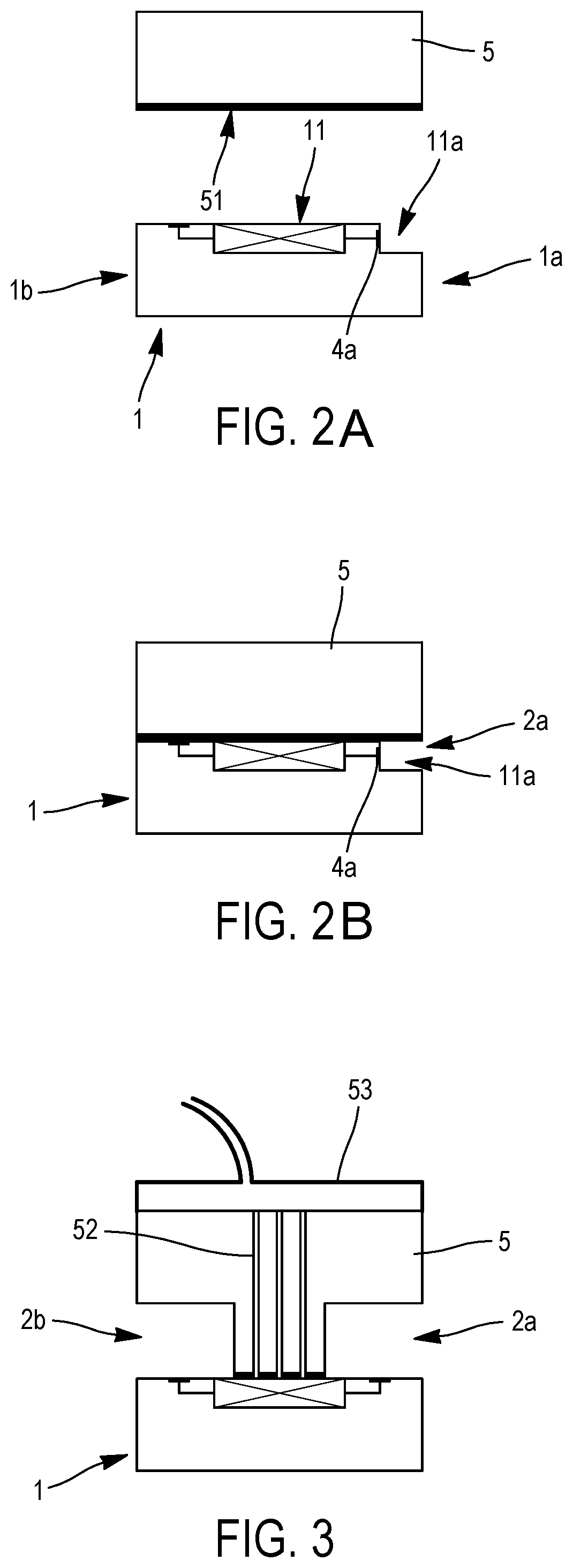
[0061]According to the present disclosure, illustrated in FIGS. 2A and 2B, the cover 5 has a flat contact face 51 and the first face 11 of the microelectronic chip 1 has at least one shoulder 11a, to form the temporary groove 2a lateral with the flat contact face 51 of cover 5. The connection terminal 4a can, in this embodiment, be designed in such a way that it leads to the first flank, in the plane of the first face 11, of the shoulder 11a (not shown) or to the other substantially vertical flank of the shoulder 11a (as shown in FIGS. 2A and 2B).

[0062]According to an advantageous variant (not shown), the first side 11 of the microelectronic chip 1 has two shoulders along each of its lateral faces 1a, 1b to form two parallel temporary lateral grooves 2a, 2b, with the flat contact face 51 of the cover 5.

[0063]Of course, the first side 11 of chip 1 may alternatively have any number of shoulders, capable of forming temporary grooves, each arranged in any orientation.

[0064]According to ...


PUM


Abstract

A method for joining a microelectronic chip to at least one wire element comprises a first step of applying a cover to a first face of the microelectronic chip, the cover being configured to form, with the first face, at least one temporary side groove. The method additionally comprises a step of inserting the wire element into the temporary groove. The method further comprises a step of attaching the wire element to the microelectronic chip. The method additionally comprises a step of removing the cover from the microelectronic chip.

Description

CROSS-REFERENCE TO RELATED APPLICATIONS[0001]This application is a national phase entry under 35 U.S.C. § 371 of International Patent Application PCT / FR2018 / 050955, filed Apr. 16, 2018, designating the United States of America and published as International Patent Publication WO 2018 / 193198 A1 on Oct. 25, 2018, which claims the benefit under Article 8 of the Patent Cooperation Treaty to French Patent Application Ser. No. 1753404, filed Apr. 19, 2017.TECHNICAL FIELD[0002]The present disclosure relates to a process for assembling a microelectronic chip on a wire element. It finds an exemplary application in the field of RFID (“Radiofrequency Identification”) electronic tagging to directly associate an antenna with a transmission chip and provide a particularly small radiofrequency device by simple manufacture. This device can be integrated into a textile thread and this thread itself can be integrated into a wide variety of objects for the identification, tracking, and administration ...

Claims


Application Information

Patent Timeline
Patent Type & Authority Patents(United States)
IPC IPC(8): H01L21/67H01L23/00H01L21/683
CPCH01L24/85H01L21/67138H01L21/6838H01L24/78H01L2224/85005H01L2224/8521H01L2224/8592H01L2224/85234H01L2224/85815H01L21/50H01L23/49811D10B2401/18D02G3/441H01L2224/48
Inventor ROLLAND, DELPHINEMACKANIC, CHRISTOPHERANDIA VERA, GIANFRANCOARENE, EMMANUEL
Owner PRIMO1D
Learn More