Unscanned optical inspection system using a micro camera array

Active Publication Date: 2021-10-19
RAMONA OPTICS INC
View PDF6 Cites 0 Cited by
  • Summary
  • Abstract
  • Description
  • Claims
  • Application Information

AI Technical Summary

Benefits of technology

[0051]The current invention leverages the technology and market trends in digital cameras and computers where digital image sensor costs have dropped exponentially as production scales have ramped for digital cameras used in consumer products. Small, low power, high pixel density image sensors are becoming increasingly common in cellphones, laptops, and in-home appliances. The invention outlined makes use of the same, or similar sensors as the ones included in consumer electronics to substantially drive down the cost of inspection equipment. However, it is clearly the intent of this patent to also claim the use of specialized imagers as there may be products that require special imaging capabilities such as very high speed, low light or depth readout from time of flight measurement. In such cases, special imagers may be used, but in most scenarios more common imagers—typically produced in high volumes for end use in consumer electronic products—will suffice.
[0052]Computational bandwidth and networking costs also continue to plummet. These trends are expected to continue such that the use of a large number of cameras, which would have been economically impractical a few years ago, is now quite reasonable and will only get less costly with time. Similarly, the computational bandwidth required to manage Gigapixel images and the computational power are decreasing with the rise of computationally efficient image processing algorithms. As detailed above, the image processing in the MCAM stageless inspection system can be done on-line or off-line depending on the needs of the customer.
[0053]By eliminating the large distance motion subsystem numerous benefits can be obtained. These include cost reduction and reduction in system weight and footprint. Also, performance is increased in higher throughput, as a single “snapshot” can be taken of the product and the entire product is imaged at once rather than having to move the camera multiple times for taking multiple individual images.
[0054]Additionally, multi-camera arrays offer other unique advantages. These include a large depth of focus than single-lens systems, and most critically enable each individual micro-camera to be brought into focus on a separate plane, to ensure that curved samples can be captured in sharp focus across the entire sample area without requiring any motion subsystems (i.e., a sample stage or imaging system stage), via one or more of the three “refocusing strategies” outlined above. The present invention's “refocusing strategies” also enable 3D imaging capabilities, by acquiring one or more images from each camera within the array under different imaging parameters (i.e., different refocusing strategy settings). For 3D imaging, the MCAM can be configured, if the operator chooses to do so, to extract the depth information within the imaged area with one image per micro-cameras within the array

Problems solved by technology

There are currently few lenses and digital image sensors that can capture this many resolvable spots, which thus presents a challenge to designing an imaging system that can capture all of this information without mechanically scanning either the sample via a sample stage or the imaging system via an imaging system stage.
Currently, however, creating an unscanned optical inspection system that can be applied to both life sciences, industrial applications, and other large scale imaging tasks remains an open challenge.
The resulting technical restrictions, including the cost, size weight, vibration damping requirements and the limitations of using a single image sensor in this approach also limit the commercial utility of the tool.
While Asar notes the value of having a fixed camera image a fixed item, today, as electrical components are decreasing in size, this resolution may be insufficient to detect smaller flaws.
These had limitations due to the large size of the cameras and required mirrors and camera mounting off the vertical axis.
This approach, however, still requires movement of the camera or the item and

Method used


Image

  • Unscanned optical inspection system using a micro camera array
  • Unscanned optical inspection system using a micro camera array
  • Unscanned optical inspection system using a micro camera array

Examples


examples

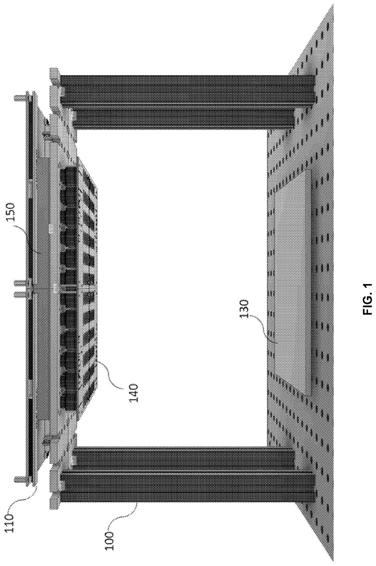
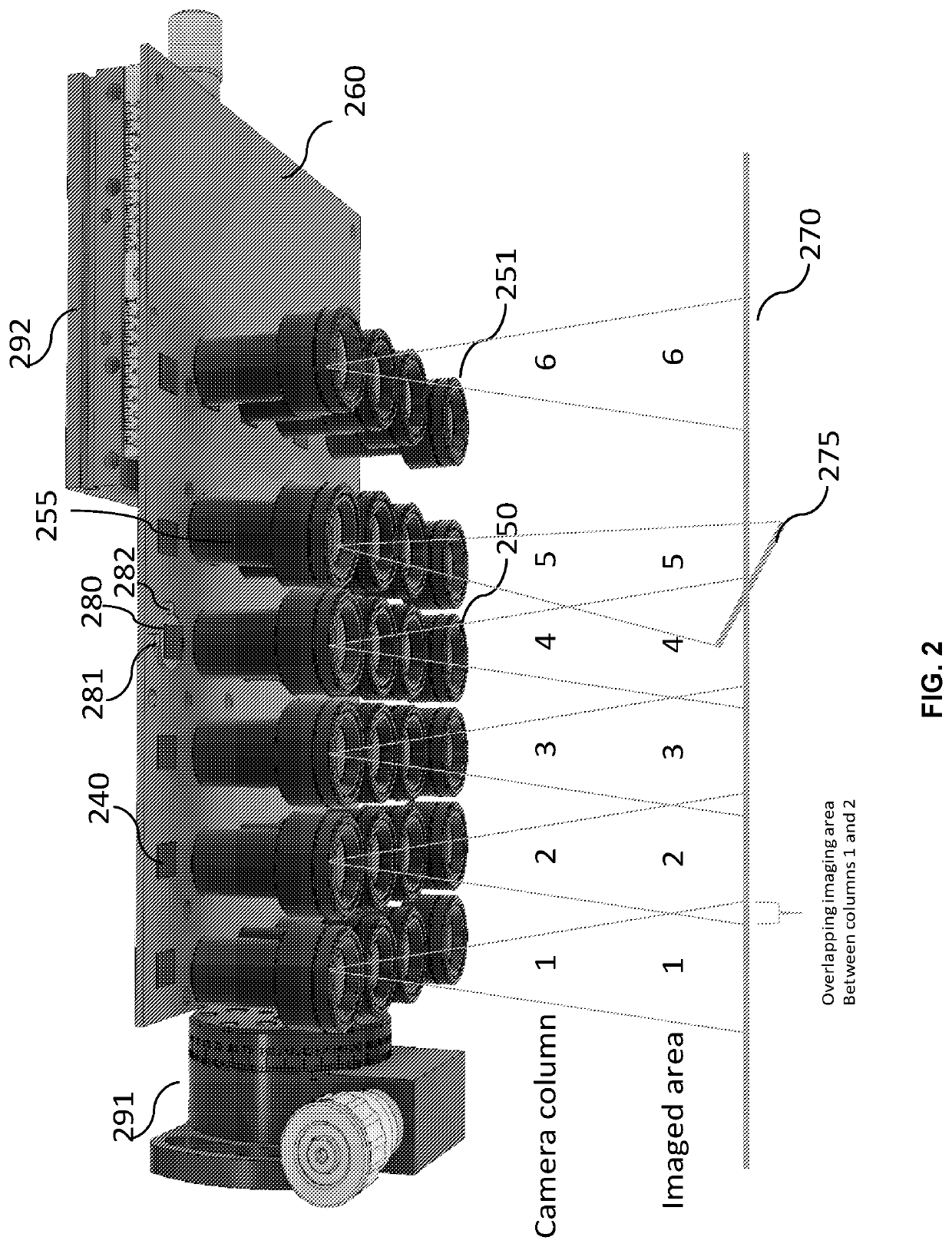
[0097]Here we provide 4 example embodiments: the first for imaging PCB over an area as large as 9×12 inches. The second and 3rd are designed to image wafers 12 inches (300 mm) in diameter. The fourth example is specifically designed for imaging biological samples located in 96 well plate configuration. For brevity, all imaging systems describe herein have 10 um resolution. For a lens with a 25 mm focal length, an f / # of 2.5, and a focal plane 225 mm away from the pupil of the lens, the system will have a magnification of 0.8×. If a 20 megapixel imaging sensor is used in each micro-camera (1 um pixel size, 5216×3896 arrangement in each sensor), then each micro camera will image an area of 41.6×31.2 mm at the imaging plane.

[0098]To image a continuous area of 9×12 inches, (approximately 228.6×304.8 mm), one would be required to tile 10×13 sensors each separated by 25 mm. For one snapshot acquisition of the system, assuming 8 bits are detected per image sensor, this corresponds to 2.6 g...


PUM


Abstract

An arrangement of one or more micro cameras are used in conjunction with computer controlled illumination to create a high-throughput microscope able to operate without the need of expensive scanning stages. A single unit contains a plurality of sensors, lenses tiled in such a way to cover a significant fraction of the desired field of view in a digital single acquisition. Mechanical stages and patterned illumination can then be used in conjunction with the system to enhanced the imaged depth of field, or create an acquisition stack to enhance the information acquired. Multiple units can be combined to obtain images of a single sample from different angles. The absence of mechanical stages makes the imaging system ideal for use in scenarios that require the sample to be in a climate and/or environmentally controlled chamber.

Description

TECHNICAL FIELD[0001]This invention relates primarily, but not exclusively, to Life Sciences and biological research tools and product inspection systems for the semiconductor, printed circuit board and electronics assembly industries. More particularly, the present invention relates to High Throughput (HTP) image scanners for multi well plates and scanning optical microscopes for life science research in live cell imaging, drug discovery and genetic research, scanning microscopes for digital pathology studies and automated defect inspection systems for bare and patterned wafers, displays, PCB's and other electronic parts and assemblies.BACKGROUND ART[0002]Electronics have become an important and ubiquitous part of modern society. Electronic products are based on semiconductor devices which are assembled with other devices on printed circuit boards to create systems that perform useful functions.[0003]The process of making the semiconductor device and the process of assembling the d...

Claims


Application Information

Patent Timeline
IPC IPC(8): H04N5/247H04N5/232G01B11/245H04N5/225
CPCH04N5/247G01B11/245H04N5/2253H04N5/23299G01N21/8806H04N23/90H04N23/54H04N23/695
Inventor HARFOUCHE, MARKHORSTMEYER, ROARKEHORSTMEYER, ROBERT
Owner RAMONA OPTICS INC
Why Eureka
Try Eureka