
Electronic apparatus and manufacturing method thereof

a manufacturing method and electronic equipment technology, applied in the field of electronic equipment, can solve the problems of increasing the size and the manufacturing cost of electronic equipment, and the difficulty of directly manufacturing active components on a substrate, thin film, or glass, and achieve the effect of losing the manufacturing cos

Active Publication Date: 2022-04-12
INNOLUX CORP
View PDF11 Cites 0 Cited by
  • Summary
  • Abstract
  • Description
  • Claims
  • Application Information

AI Technical Summary

Benefits of technology

[0009]Based on the above, the electronic apparatus and the manufacturing method of the electronic apparatus according to the embodiments of the disclosure are able to realize an electronic apparatus with an electronic structure that is smaller and requires a lost manufacturing cost by using RDL routing with a fewer number of layers and disposing a transistor circuit.

Problems solved by technology

The increasing delicacy of electronic apparatuses makes it more and more difficult to directly manufacture an active assembly on a substrate, a thin film, or glass.
Besides, due to the line width and pitch limitations in semiconductor manufacturing processes, a multi-layered routing structure needs to be manufactured on a conventional circuit substrate, so as to dispose an active assembly on the circuit substrate.
Accordingly, the size and the manufacturing cost of an electronic apparatus are increased.

Method used


Image

  • Electronic apparatus and manufacturing method thereof
  • Electronic apparatus and manufacturing method thereof
  • Electronic apparatus and manufacturing method thereof

Examples


first embodiment

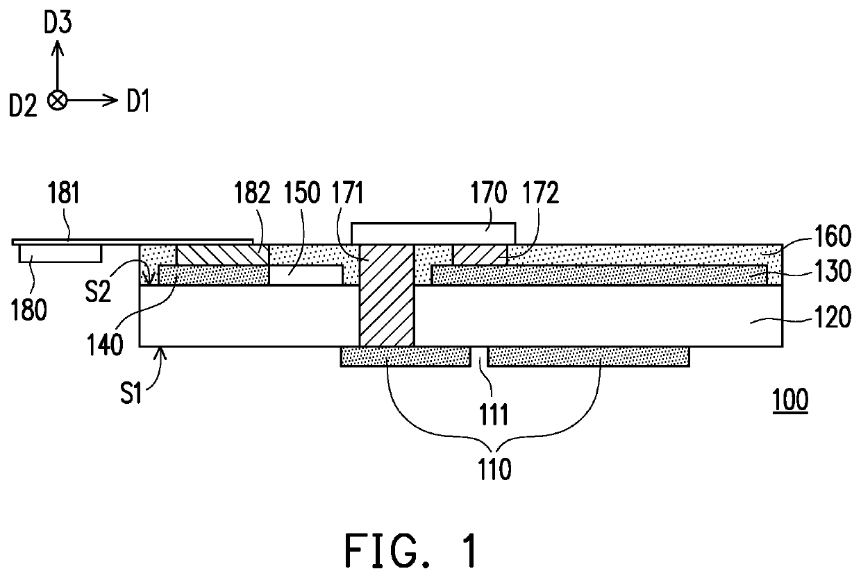
[0034]FIG. 1 is a schematic cross-sectional view illustrating a structure of an electronic apparatus according to the disclosure. Referring to FIG. 1, an electronic apparatus 100 may include an electronic structure having double-sided redistribution layer (RDL) routing, so that a relevant electronic element or circuit element may be disposed on both sides of a substrate. However, the disclosure is not limited thereto. Specifically, the electronic apparatus 100 may include a first metal layer 110, a first insulating layer 120, a second metal layer 130, a routing layer 140, a transistor circuit 150, a second insulating layer 160, an electronic assembly 170, and a control circuit 180. The transistor circuit 150 may include one or more transistors, such as a thin-film transistor (TFT), and the transistors may be bottom-gate transistors, top-gate transistors, or double / dual-gate transistors. The transistor circuit 150 may be electrically connected with the first metal layer 110 and / or th...

second embodiment

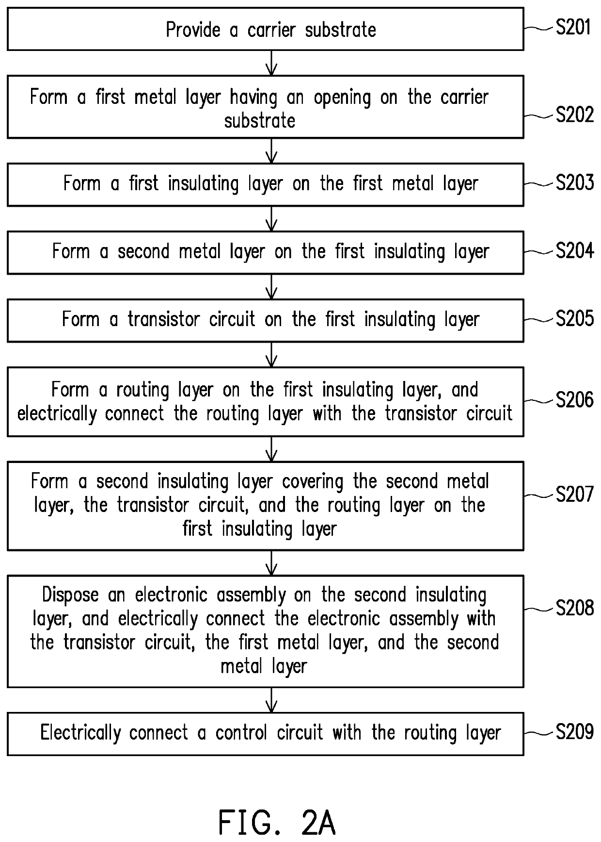
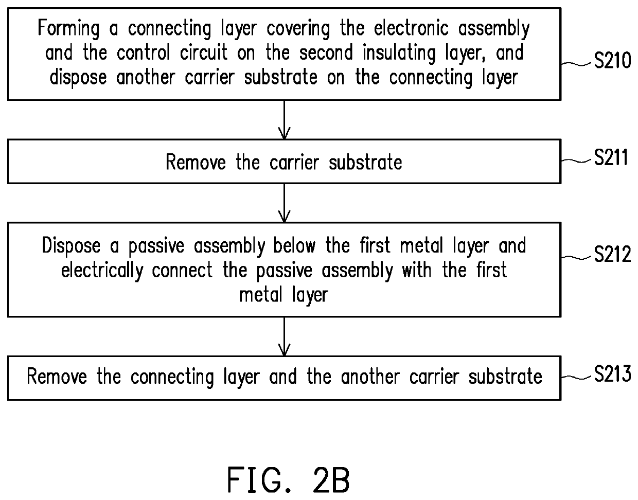
[0046]FIGS. 5A and 5B are flowcharts illustrating a manufacturing method of the electronic apparatus according to the disclosure. FIGS. 6A to 6D are schematic cross-sectional views illustrating structures in respective stages in the manufacturing method shown in FIGS. 5A and 5B. Each of the steps in the embodiment may be carried out by performing a corresponding semiconductor manufacturing process or a combination of a plurality of corresponding semiconductor manufacturing processes. In addition, the structures of FIGS. 3A to 3D formed in the respective intermediate steps may be respectively implemented independently as specific electronic apparatuses, and these structures are not limited to being only applicable to the electronic apparatus manufactured in the final step. Referring to FIGS. 5A and 6A, the manufacturing method of FIG. 5A allows to manufacture an electronic apparatus with a structure having double-sided RDL routing. In Step S501, a carrier substrate 601 is provided. T...

third embodiment

[0049]FIG. 7 is a schematic cross-sectional view illustrating a structure of an electronic apparatus according to the disclosure. Referring to FIG. 7, an electronic apparatus 700 may include an electronic structure having single-sided redistribution layer (RDL) routing, so that a relevant electronic / circuit element may be disposed on one side of a substrate. Specifically, the electronic apparatus 700 may include a first metal layer 710, a first insulating layer 720, a second metal layer 730, a routing layer 740, a transistor circuit 750, a second insulating layer 760, a PN junction assembly 770, and a control circuit 780. The transistor circuit 750 may include one or more transistors, and the transistors may be bottom-gate transistors, top-gate transistors, or double / dual-gate transistors. In the embodiment, the first insulating layer 720 includes the first surface S1 and the second surface S2. The first surface S1 is opposite to the second surface S2. In the embodiment, the first i...


PUM

PropertyMeasurementUnit
insulatingaaaaaaaaaa
widthaaaaaaaaaa
sizeaaaaaaaaaa

Abstract

The disclosure provides an electronic apparatus and a manufacturing method thereof. The electronic apparatus includes a first insulating layer, a first metal layer, a second metal layer, and an electronic assembly. The first insulating layer includes a first surface and a second surface opposite to the first surface. The first metal layer has an opening and is formed on the first surface. The second metal layer is formed on the second surface and a projection of the opening on the second surface is overlapped with a projection of the second metal layer on the second surface. The electronic assembly is electrically connected with the first metal layer and the second metal layer.

Description

CROSS-REFERENCE TO RELATED APPLICATION[0001]This application claims the priority benefit of U.S. provisional application Ser. No. 62 / 879,568, filed on Jul. 29, 2019, U.S. provisional application Ser. No. 62 / 985,892, filed on Mar. 6, 2020, and China application serial no. 202010411348.5, filed on May 15, 2020. The entirety of each of the above-mentioned patent applications is hereby incorporated by reference herein and made a part of this specification.BACKGROUNDTechnical Field[0002]The disclosure relates to an apparatus, and particularly relates to an electronic apparatus and a manufacturing method thereof.Description of Related Art[0003]The increasing delicacy of electronic apparatuses makes it more and more difficult to directly manufacture an active assembly on a substrate, a thin film, or glass. Besides, due to the line width and pitch limitations in semiconductor manufacturing processes, a multi-layered routing structure needs to be manufactured on a conventional circuit substr...

Claims


Application Information

Patent Timeline
Patent Type & Authority Patents(United States)
IPC IPC(8): H01L23/528H01L27/06H01L23/522H01L21/8234H01L29/93H01L23/538H01L21/60
CPCH01L23/5283H01L21/823475H01L23/5223H01L23/5226H01L27/0629H01L29/93H01L23/5385H01L27/0694H01L2021/6006H01L23/5386H01L21/76895H01L27/1214H01L23/5387
Inventor HUNG, TANG CHINTING, CHIN-LUNGWEI, CHUNG-KUANGKAO, KER-YIHWANG, TONG-JUNGHSIEH, CHIH-YUNGHUANG, HAO JUNGLI, I-YINHO, CHIA-CHILIN, YI HUNGCHOU, CHENG-HSUTSENG, CHIA-PING
Owner INNOLUX CORP
Learn More