
SPAD device for excess bias monitoring

a technology of bias monitoring and spad, which is applied in the direction of optical radiation measurement, instruments, photometry, etc., can solve the problem that light sources may not be easily available for some types of applications

Active Publication Date: 2022-06-07
AMS AG
View PDF13 Cites 0 Cited by
  • Summary
  • Abstract
  • Description
  • Claims
  • Application Information

AI Technical Summary

Problems solved by technology

A low dark count rate is desired, but it causes tardy triggering and may therefore prevent the undelayed control of the excess bias voltage.
Faster triggering for calibration can be enabled by the use of a light source to illuminate the single-photon avalanche diode, but a light source may not be easily available for some types of applications.

Method used


Image

  • SPAD device for excess bias monitoring
  • SPAD device for excess bias monitoring
  • SPAD device for excess bias monitoring

Examples


Embodiment Construction

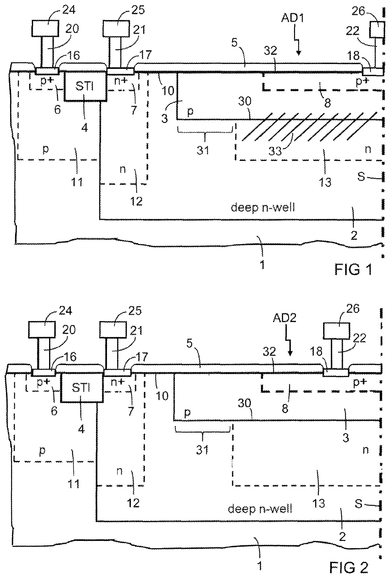
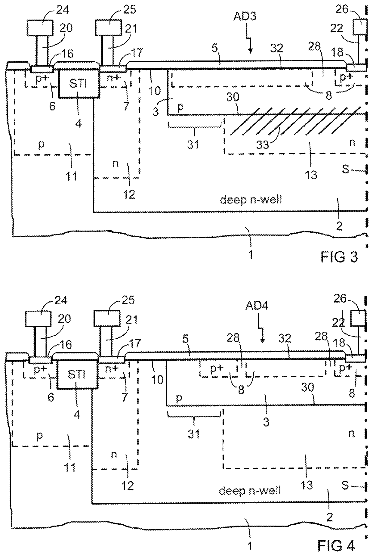
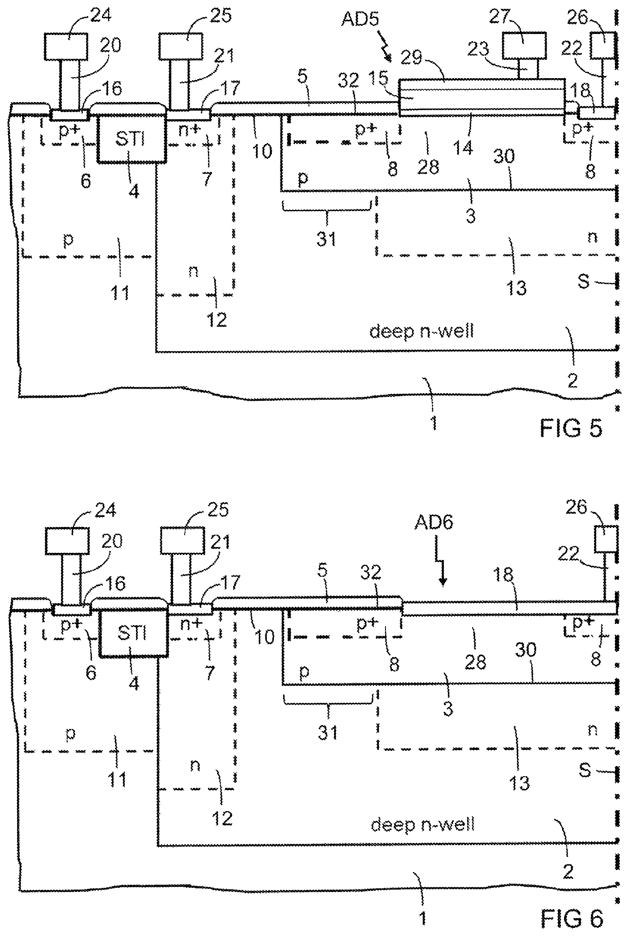
[0035]FIG. 1 is a partial cross section of a single-photon avalanche diode AD1 with relatively high dark count rate. The single-photon avalanche diode AD1 need not be symmetrical, but it may comprise a symmetry. A rotational symmetry is indicated in the figures by the symmetry axis S as an example. The other appended figures show the same portion of the single-photon avalanche diode, so that the differences between the embodiments are evident.

[0036]The single-photon avalanche diode AD1 comprises a substrate 1 of semiconductor material, which may be silicon, for instance. Doped regions in the substrate 1 have a first type of conductivity or an opposite second type of conductivity. The first type of conductivity may be p-type conductivity, so that the second type of conductivity is n-type conductivity, as indicated in the figures by way of example. The types of conductivity may be reversed. Doping concentrations for either type of conductivity that are sufficiently high for the format...


PUM

PropertyMeasurementUnit
temperatureaaaaaaaaaa
temperaturesaaaaaaaaaa

Abstract

The SPAD device comprises a single-photon avalanche diode and a further single-photon avalanche diode having breakdown voltages, the single-photon avalanche diodes being integrated in the same device. The breakdown voltages are equal or differ by less than 10%. The single-photon avalanche diode is configured to enable to induce triggering or to have a dark count rate that is higher than the dark count rate of the further single-photon avalanche diode.

Description

[0001]The present disclosure is related to single-photon avalanche diodes.BACKGROUND OF THE INVENTION[0002]Single-photon avalanche diodes (SPADs) are semiconductor devices with a p-n junction. A reverse bias is used to increase the width of the depletion region. When the operating voltage providing the reverse bias exceeds the breakdown voltage of the p-n junction by the so-called excess bias voltage, a single charge carrier injected into the depletion layer triggers a self-sustaining avalanche. The current rises swiftly unless the operating voltage is decreased to the breakdown voltage or below. The avalanche is initiated by pairs of electrons and holes, which are generated by photons from a light source or by a forward biased p-n junction.[0003]The breakdown voltage changes with temperature and can be different for individual devices at the same temperature because of tolerances of the manufacturing process. It is important to control the excess bias voltage by a suitable circuit,...

Claims


Application Information

Patent Timeline
Patent Type & Authority Patents(United States)
IPC IPC(8): H01L31/02H01L31/0352H01L31/107
CPCH01L31/02027H01L31/035272H01L31/107H01L27/1443G01J2001/4466
Inventor RÖHRER, GEORGKAPPEL, ROBERTLILIC, NENAD
Owner AMS AG
Learn More