
Single-photon avalanche diode with low dark counting rate and manufacturing method thereof

A technology of single-photon avalanche and count rate, which is applied in the field of single-photon detection, can solve the problems of high electric field in the avalanche area, high dark count rate of devices, high doping level of single-photon avalanche diodes, etc., to suppress the tunneling effect and reduce the electric field Effect

Inactive Publication Date: 2020-08-04
CHINA JILIANG UNIV
View PDF4 Cites 0 Cited by
  • Summary
  • Abstract
  • Description
  • Claims
  • Application Information

AI Technical Summary

Problems solved by technology

The single photon avalanche diode with this structure has a high doping level, which leads to an excessively high electric field in the avalanche region, and the avalanche is accompanied by the tunneling effect, which makes the dark count rate of the device very large

Method used


Image

  • Single-photon avalanche diode with low dark counting rate and manufacturing method thereof
  • Single-photon avalanche diode with low dark counting rate and manufacturing method thereof
  • Single-photon avalanche diode with low dark counting rate and manufacturing method thereof

Examples


Embodiment Construction

[0035] In order to better understand the content of the patent of the present invention, the technical solution of the present invention will be further described below in conjunction with the accompanying drawings.

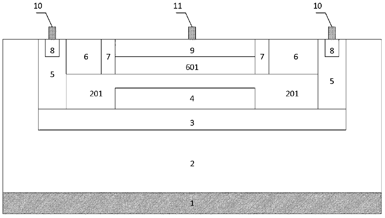
[0036] Such as figure 1 As shown, the single photon avalanche diode with low dark count rate includes a P-type epitaxial layer 2 arranged on a substrate 1, an N-type isolation region 3 is arranged inside the P-type epitaxial layer 2, and both sides of the N-type isolation region 3 are symmetrically arranged N-well region 5, the top of N-well region 5 is coaxially provided with N+ heavily doped region 8, the center N-type region 4 is coaxially arranged above the N-type isolation region 3, and the P-well region 6 is arranged above the center N-type region 4. A P+ heavily doped region 9 is arranged coaxially inside the P well region 6 , and a P-type guard ring region 7 is arranged symmetrically on both sides of the P+ heavily doped region 9 .

[0037] The central r...


PUM


Abstract

The invention discloses a single-photon avalanche diode with a low dark counting rate and a manufacturing method thereof, which belong to the technical field of single-photon detection. The single-photon avalanche diode comprises a P-type epitaxial layer arranged on a substrate; an N-type isolation region is arranged in the P-type epitaxial layer; N well regions are symmetrically arranged on the two sides of the N-type isolation region; an N + heavily doped region is coaxially arranged at the top of the N well regions; a central N-type region is coaxially arranged above the N-type isolation region; a P well region is arranged above the central N-type region; a P + heavily doped region is coaxially arranged in the P well region; and P-type protection ring regions are symmetrically arrangedon the two sides of the P + heavily doped region. According to the invention, the P well central region, the P-type epitaxial layer central region and the central N-type region are adopted to form anavalanche region, so that the electric field of the avalanche region is reduced, the tunneling effect is inhibited, and the dark counting rate of the device is remarkably reduced.

Description

technical field [0001] The invention belongs to the technical field of single photon detection, and in particular relates to a low dark count rate single photon avalanche diode and a manufacturing method thereof. Background technique [0002] Single-photon detection technology has broad application prospects in the fields of national defense construction, industry and civilian life, such as: fluorescence lifetime imaging, radar ranging, three-dimensional vision systems and quantum key learning. As a core device for single photon detection, single photon avalanche diode (single photon avalanche photodiode, denoted as SPAD) based on CMOS technology has attracted more and more attention and attention of researchers. The single photon avalanche diode in Geiger mode is a detector that can detect extremely weak light signals. It has large internal gain, high sensitivity, fast response speed, high detection efficiency, low noise, small size, strong structure and easy integration. ...

Claims


Application Information

Patent Timeline
IPC IPC(8): H01L31/107H01L31/0352H01L31/18
CPCH01L31/035272H01L31/107H01L31/1804Y02P70/50
Inventor 赵天琦储童冯桂兰林春兰
Owner CHINA JILIANG UNIV
Learn More