Semiconductor device

a semiconductor device and semiconductor technology, applied in semiconductor devices, semiconductor/solid-state device details, power conversion systems, etc., can solve the problems of cracks, increase in the dimension of the semiconductor device, and decrease in the withstanding or breakdown voltage of the semiconductor switch

Inactive Publication Date: 2002-12-05
HITACHI LTD
View PDF0 Cites 33 Cited by
  • Summary
  • Abstract
  • Description
  • Claims
  • Application Information

AI Technical Summary

Problems solved by technology

The former approach is generally encountered with risks as to decreases in withstanding or breakdown voltage of semiconductor switches, which in turn strictly requires suppression of an increase in voltage being applied to a semiconductor switch during turn-off operations thereof to less than or equal to the breakdown level thereof.
On the contrary, the latter approach suffers from increase in semiconductor switch mount area and also increase in wiring lead area, which would result in an increase in dimension of the semiconductor device.
In addition, due to the so-called temperature cycling occurring during start-up and shut-down of the semiconductor device due to the presence of differences in thermal expandabilities of constituent parts or components such as the semiconductor switches, dielectric substrate and heat sink plate or else, distortion can take place at soldered contact portions between the semiconductor switches and the dielectric substrate and also at wire-bonding portions of such semiconductor switches, which leads to creation and growth of cracks through repeated experience of the temperature cycle.
In particular, advanced semiconductor devices with enhanced performance for achievement of large-current switchabilities do not come without accompanying penalties as to either soldering cracks or accidental bond-wire breaking due to thermal stresses in the way stated previously, resulting in a likewise decrease in lifetime thereof.

Method used


Image

  • Semiconductor device
  • Semiconductor device
  • Semiconductor device

Examples


first embodiment

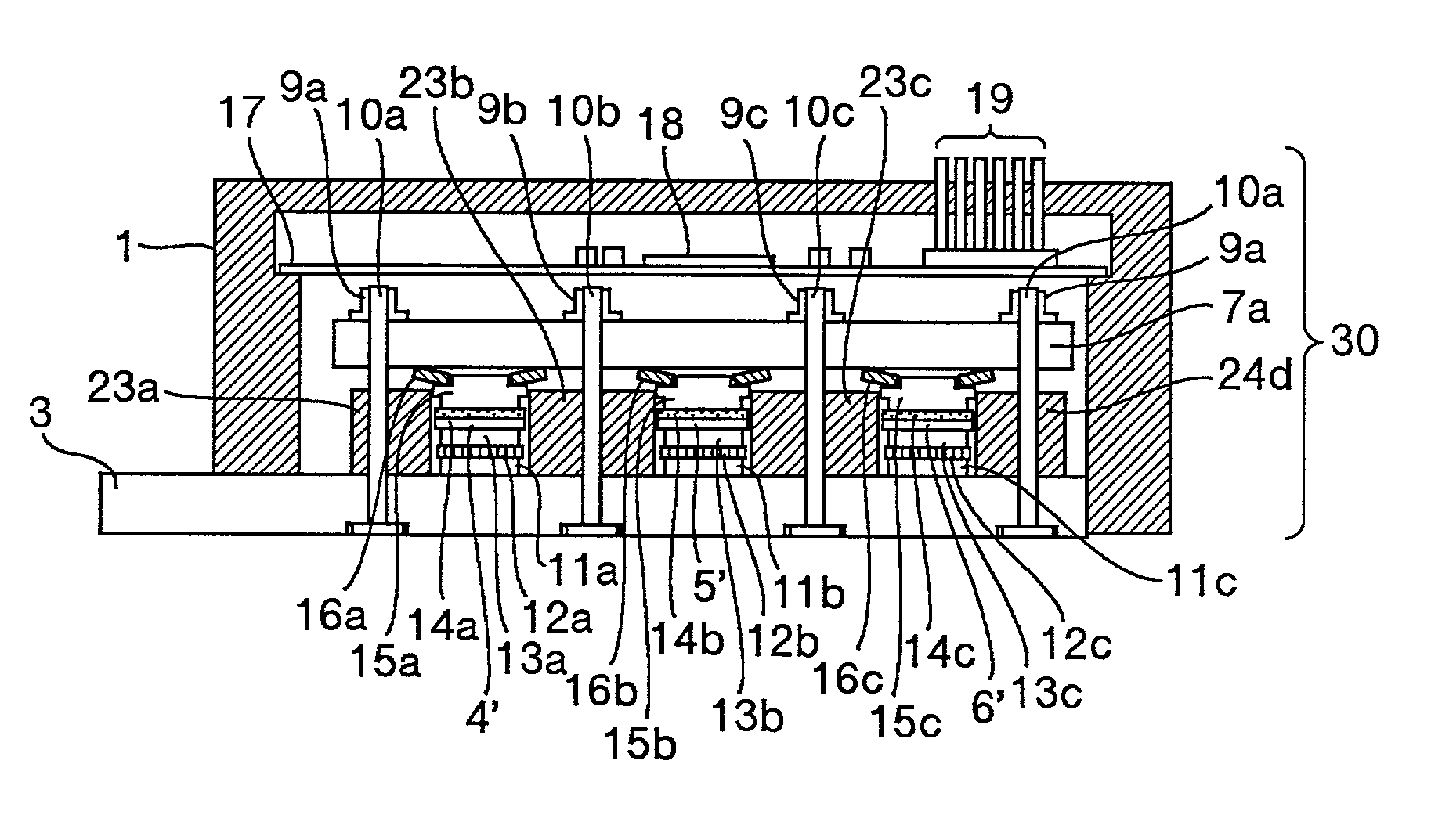
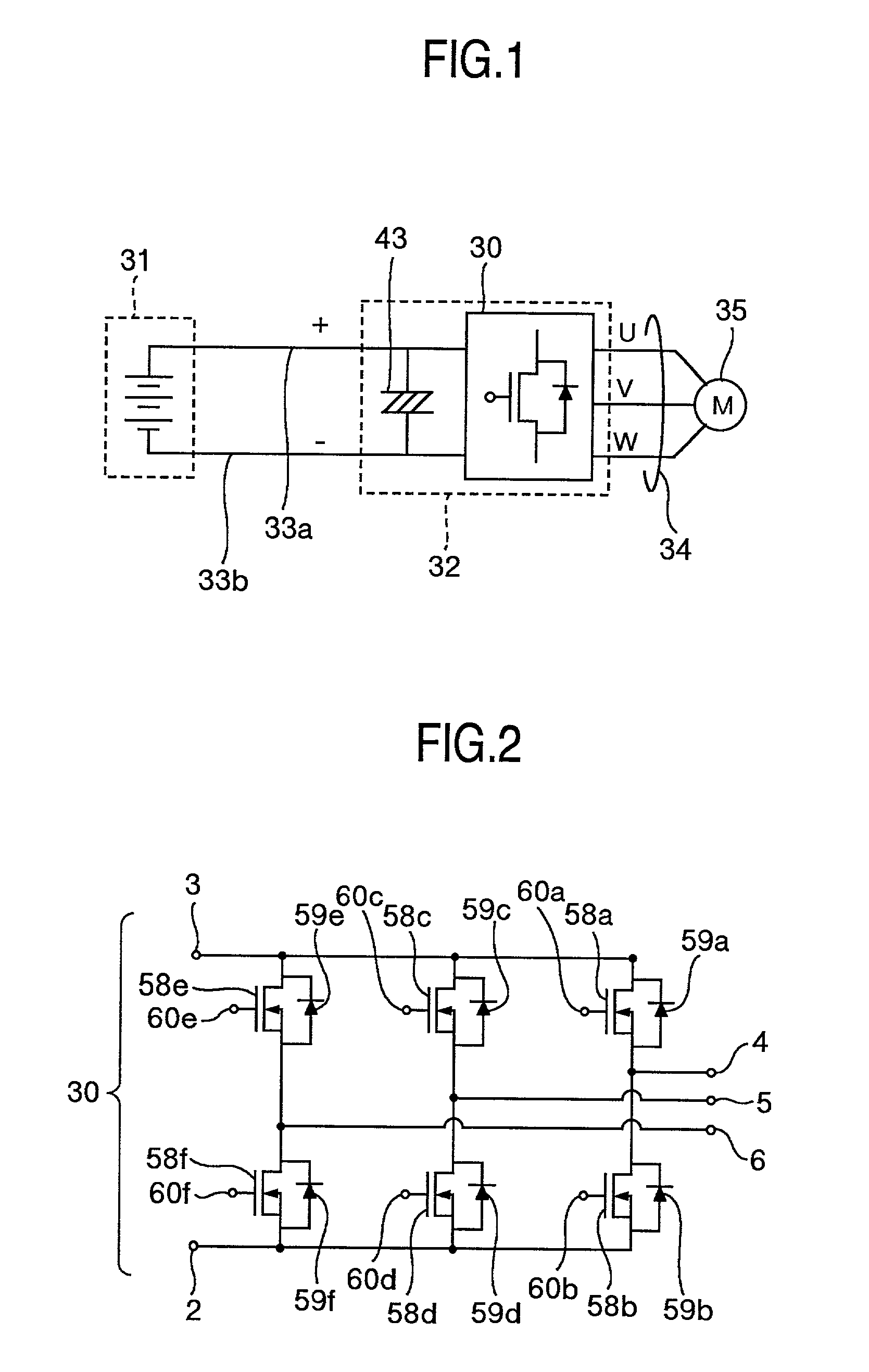
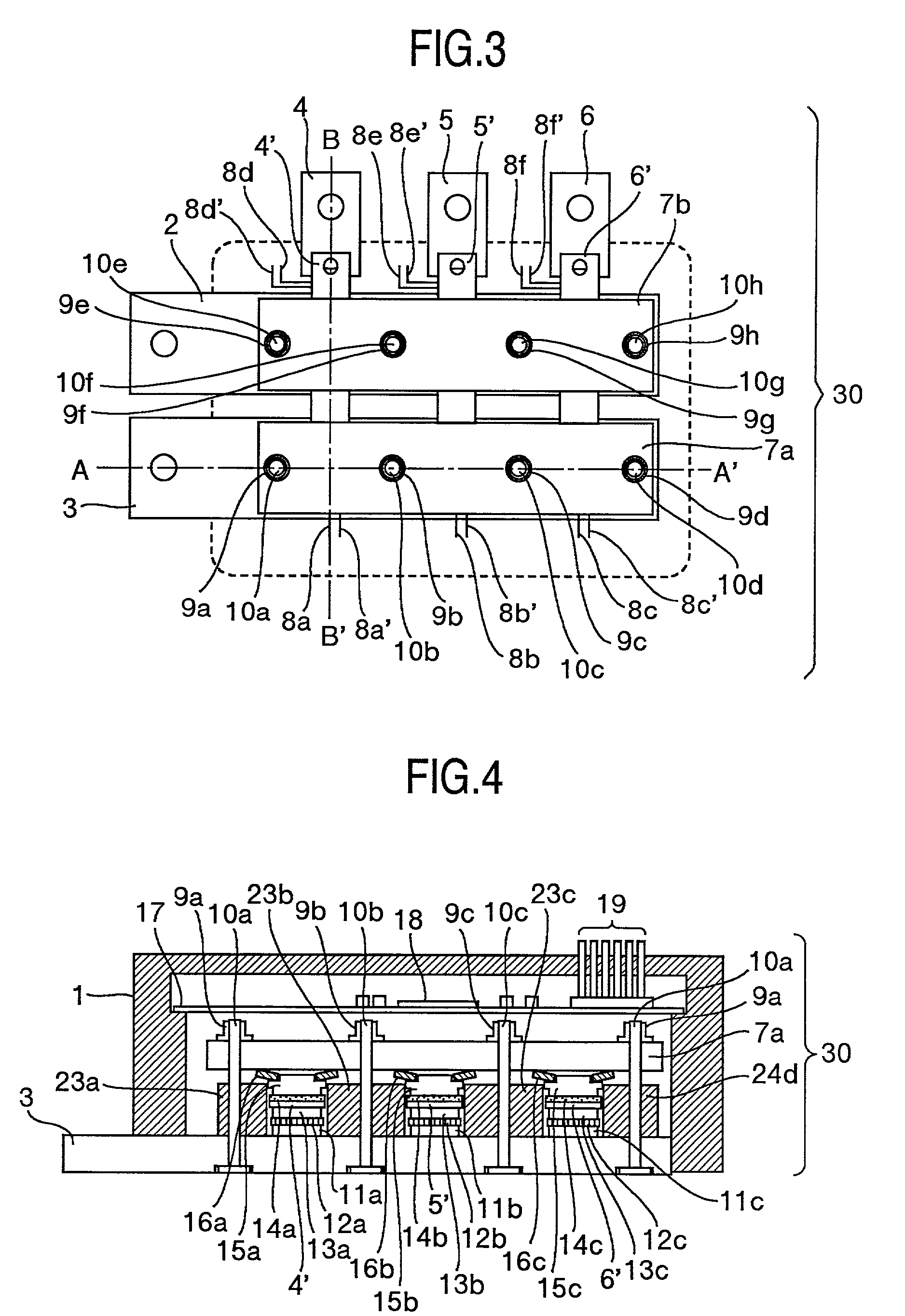
[0045] FIGS. 3 to 5 are diagrams showing a semiconductor device in accordance with the invention, wherein FIG. 3 depicts a top view; FIG. 4 is a cross-sectional view as taken along line A-A' of FIG. 3; and, FIG. 5 is a sectional view taken along line B-B' in FIG. 3. In FIG. 3, numeral 1 designates a package housing or casing; 2 denotes a negative polarity DC wiring board or plate; 3 is a positive polarity DC wiring plate; 4, 5, 6, 4', 5' and 6' are output wiring plates; 7a-7b, pressure applying or "pressurization" plates; 8a to 8f and 8a'-8f', signal transfer lines formed of electrical leads; 9a-9f, collars; 10a-10f, bolts; 30, semiconductor device. Each DC terminal 2, 3 is provided with a through-going hole for wiring attachment to a DC power supply unit. Respective output wiring plates 4-6 are provided holes for output wiring attachment. Signal wiring leads as used herein are organized into pairs; for example, wiring leads 8a and 8a' are designed as a pair with one being connected...

second embodiment

[0062] FIGS. 6 to 8 are diagrams showing a semiconductor device in accordance with the invention, wherein FIG. 6 is a top plan view, FIG. 7 is a sectional view taken along line A-A' of FIG. 6, and FIG. 8 is a sectional view along line B-B1 of FIG. 6. In FIG. 6, reference character 1' designates a casing; 2 denotes a negative DC wiring plate; 3 is a positive DC wiring plate; 4 to 6, output wiring plates; 7a-7c, pressurization plates; 8a-8f and 8a'-8f', signal transmission lines formed of conductive wiring leads; 10a-10c, bolts; 72a-72c, nuts; 24a-c, insulators; 25, printed wiring plate; 30, semiconductor device. Each wiring plate 2, 3 is provided with openings or holes for lead attachment to the DC power supply. Each output wiring plate 4, 5, 6 has a hole for output lead attachment. The signal leads are organized into pairs; for example, leads 8a and 8a' are paired for connection to the gate electrode and source electrode of a MOSFET for use as one semiconductor switch.

[0063] In FIG....

third embodiment

[0069] FIGS. 9 and 10 are diagrams showing a semiconductor device in accordance with the invention, wherein FIG. 9 is a top plan view, and FIG. 10 is a sectional view taken along line A-A' of FIG. 9. In FIG. 9, reference character 1' designates a casing; 2 and 2a-2c denote negative DC wiring plates; 3 is a positive DC wiring plate; 4-6 and 4'-6', output wiring plates; 7a-7f, pressurization plates; 8a-8f and 8a'-8f', signal transmission lines formed of wiring leads; 10a-10k and 10m-10n, bolts; 72a-72k and 72m-n, nuts; 22a-f, screws; 30, semiconductor device. Each wiring plate 2, 3 is provided with more than one hole for lead attachment to the DC power supply. Output terminals of the wiring plates 4-6 are provided with holes for output lead attachment. The signal leads are organized into pairs; for example, leads 8a and 8a' are paired for connection to the gate electrode and source electrode of a MOSFET for use as one semiconductor switch.

[0070] In FIG. 10, 1 indicates the casing; 2, ...


PUM


Abstract

A semiconductor device including a positive polarity wiring plate, negative wiring plate, more than one output wiring plate, semiconductor switch element and conductive buffer or "cushion" member is disclosed. The semiconductor switch element and cushion member are compressively interposed between the output wiring plate and positive wiring plate and also between the output wiring plate and negative wiring plate to thereby constitute bridge circuitry. The positive wiring plate, negative wiring plate or output wiring plate is for use as one support body of a pressurization structure. With such an arrangement, it is possible to improve the heat releasability of semiconductor elements while at the same time reducing the inductance of direct current (DC) circuitry to thereby suppress heat generation of the semiconductor elements, thus increasing the reliability relative to temperature cycles.

Description

[0001] 1. Field of the Invention[0002] The present invention relates generally to semiconductor devices and, more particularly, to a semiconductor device with heat generation suppressibility and enhanced heat releasability for improving the reliabilty relative to temperature cycles.[0003] 2. Description of the Related Art[0004] FIG. 21 is a diagram showing a parts-mounting structure of a prior known semiconductor device with built-in bridge circuitry including semiconductor switch elements. In this drawing, reference numeral "1" designates an enclosure called the package housing or simply casing; 2 denotes a negative polarity direct current (DC) wiring plate; 3 indicates a positive polarity DC wiring plate; 4 is a U-phase output terminal; 5, V-phase output terminal; 6, W-phase output terminal; 12a and 12d, semiconductor switches; 30, semiconductor device; 61, dielectric substrate; 62a, 62b, 62c, 62d, 62e, wiring leads; 67, heat radiation plate, also known as "heat sink." The semicon...

Claims


Application Information

Patent Timeline
Patent Type & Authority Applications(United States)
IPC IPC(8): H01L23/48H01L23/40H01L25/11H02M7/48H02M7/5387
CPCH01L24/72H01L25/162H01L2924/1305H01L2924/1306H01L2924/01047H01L2924/01004H01L2924/01013H01L2924/01029H01L2924/01033H01L2924/01039H01L2924/01042H01L2924/01074H01L2924/01082H01L2924/13055H01L2924/13091H01L2924/14H01L2924/19041H01L2924/19043H01L2924/30105H01L2924/30107H01L2924/01005H01L2924/01006H01L2924/01023H01L2924/00H01L2924/351H01L2924/181
Inventor SHIRAKAWA, SHINJIMISHIMA, AKIRAMASHINO, KEIICHIINNAMI, TOSHIYUKIANAN, HIROMICHIOCHIAI, YOSHITAKA
Owner HITACHI LTD
Why Eureka
Try Eureka