Intelligent blemish control algorithm and apparatus

a blemish control algorithm and intelligent technology, applied in the field of digital image processing, can solve problems such as the visual effect of bad pixels being very annoying, the output of a ccd/cmos sensor subject to artifacts, and the pixel defects of solid-state sensors such as ccd/cmos sensors are common problems

Inactive Publication Date: 2002-12-26
ESS TECH INT INC +1
View PDF11 Cites 91 Cited by
  • Summary
  • Abstract
  • Description
  • Claims
  • Application Information

AI Technical Summary

Problems solved by technology

Pixel defects in solid-state sensors such as CCD / CMOS sensors have been a common problem.
The output from a CCD / CMOS sensor is subject to artifacts due to bad pixels.
The visual effect of bad pixels can be very annoying as bad pixels manifest as black, white or gray dots in captured images.
With sensor sizes increasing into the mega-pixel range, pixel defects are almost inevitable.
Because it is very hard to produce defect-free sensors, it has been common practice for CCD / CMOS sensor manufacturers to market sensors with a small amount of defective pixels.
If the record is lost, however, the sensor device must be re-tested to obtain the locations of the bad pixels.
According to one model, there are three types of pixel defects: stuck high, stuck low and abnormal sensitivity.
To further illustrate, a pixel with the stuck high defect manifests itself as a very noticeable artifact (bright spot in a gray or dark area), which is most visually objectionable in a gray or dark area, particularly in a monochrome sensor.
The probability of finding pixel defects increases as more test pictures are used.
This process may not be desirable.
Though the method does a fairly good job alleviating the effect of defective pixels, some subtle features, however, may be altered inadvertently.
In this case, the sensor does not provide full resolution samples.
However, a defective pixel detection algorithm can result in false detections where a normal pixel is classified as a defective pixel.
Moreover, the probability of false detections increases as sensor sizes increase.

Method used


Image

  • Intelligent blemish control algorithm and apparatus
  • Intelligent blemish control algorithm and apparatus
  • Intelligent blemish control algorithm and apparatus

Examples


Embodiment Construction

[0030] With reference to the drawings, embodiments of an image processing method and apparatus, according to the present invention, is described below.

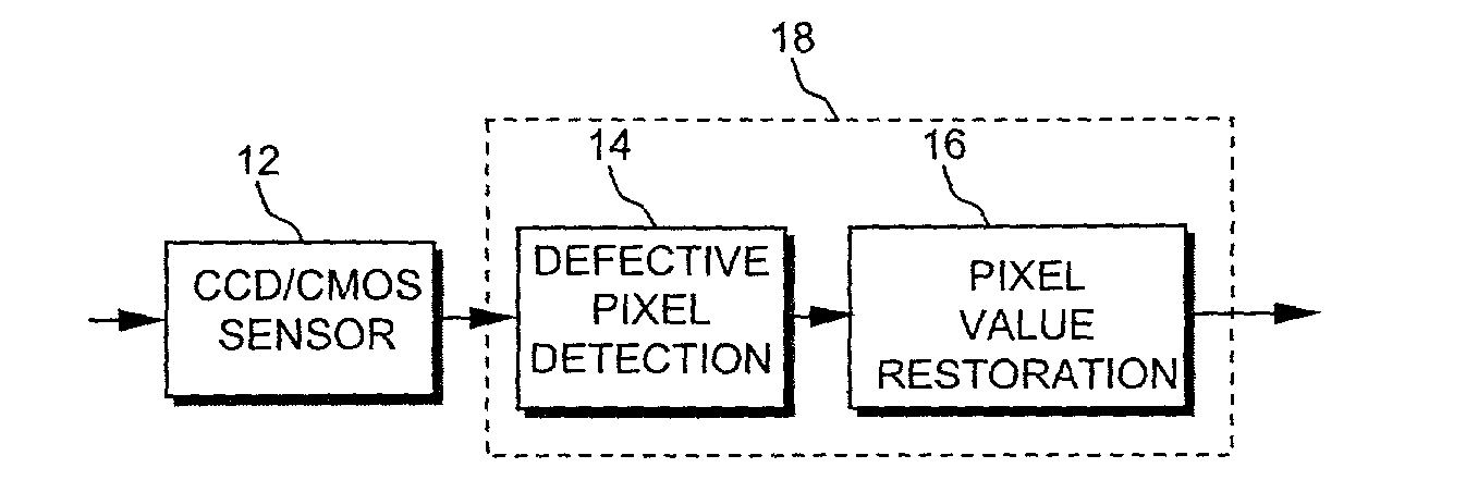
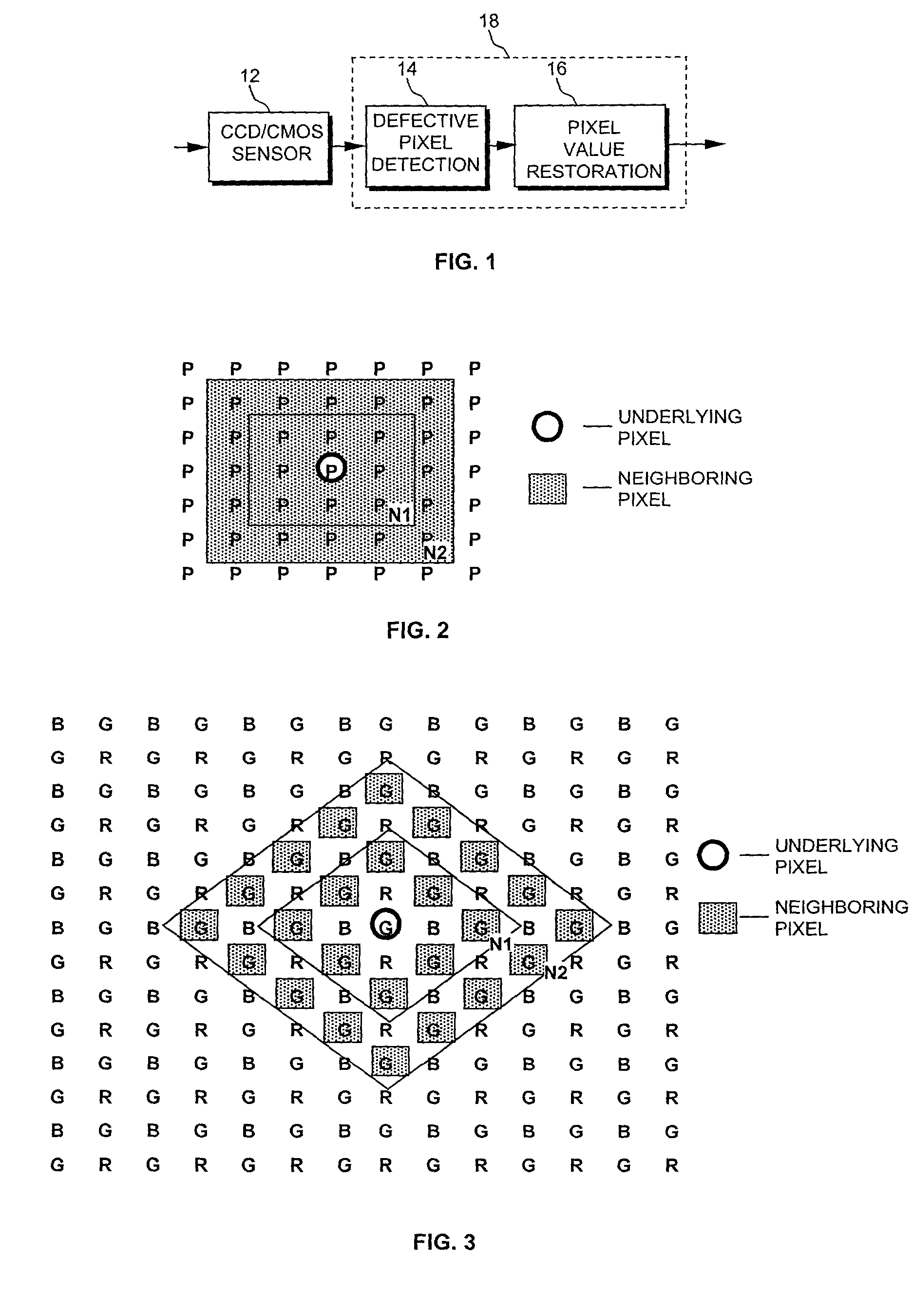
[0031] FIG. 1 shows a simplified high-level block diagram of an image processing unit 18, also referred to as an intelligent control circuit, that contains the main functional elements required to implement a blemish control algorithm, according to embodiments of the present invention. Image processing unit 18 includes a defective pixel detection stage 14 and a pixel value restoration stage 16. An output from a CCD / CMOS sensor device 12 feeds into image processing unit 18. Image processing unit 18 can operate with a CCD / CMOS sensor device in real-time, i.e., each time the CCD / CMOS feeds a new image to image processing unit 18. This means that image processing unit 18 can operate in the field well after such a sensor has been manufactured and placed into products.

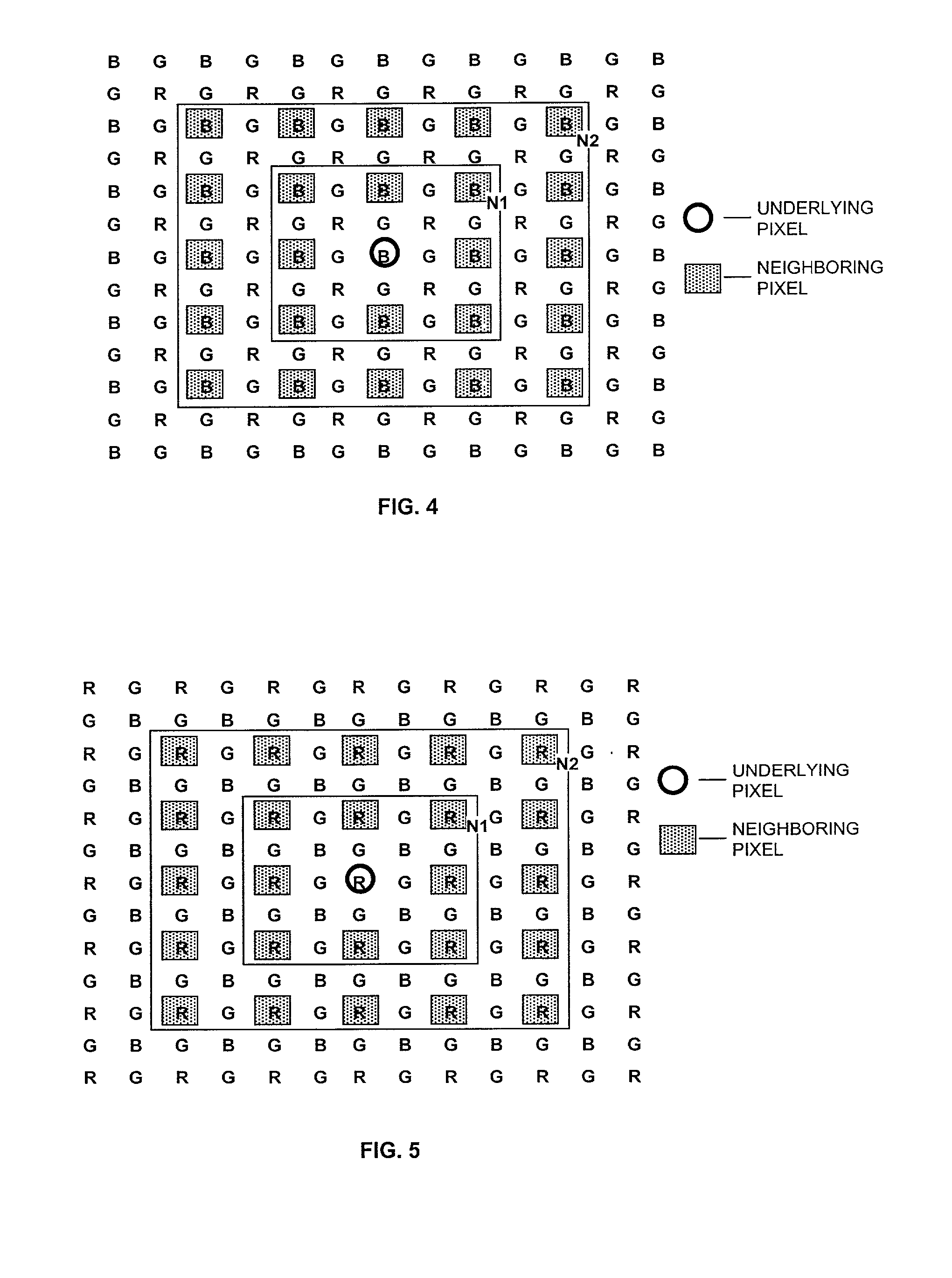
[0032] In operation, defective pixel detection stage 14 examines each pix...


PUM


Abstract

An image processing method and apparatus is described for processing a signal from a monochrome or color sensor that may be subject to pixel defects or blemishes. Without prior knowledge of any pixel defects, the processing method examines each pixel value and its neighboring pixel values. A number of tests are applied to the set of pixel values to determine whether the underlying pixel is defective. If the underlying pixel is determined to be defective, the pixel value is replaced by an estimate value derived from the values of its neighboring pixels. Otherwise, the pixel value remains intact.

Description

[0001] 1. Field of the Invention[0002] The invention relates to the field of digital image processing and more specifically to blemish control in solid-state CCD / CMOS sensors that are subject to pixel defects.[0003] 2. Description Relative to the Prior Art[0004] Pixel defects in solid-state sensors such as CCD / CMOS sensors have been a common problem. The output from a CCD / CMOS sensor is subject to artifacts due to bad pixels. The visual effect of bad pixels can be very annoying as bad pixels manifest as black, white or gray dots in captured images. With sensor sizes increasing into the mega-pixel range, pixel defects are almost inevitable. Because it is very hard to produce defect-free sensors, it has been common practice for CCD / CMOS sensor manufacturers to market sensors with a small amount of defective pixels. These slightly defective sensors are often shipped with a record listing the locations of defective pixels.[0005] Sensors with a slight defect might be tolerable for some a...

Claims


Application Information

Patent Timeline
Patent Type & Authority Applications(United States)
IPC IPC(8): H04N5/217H04N5/367H04N5/369
CPCH04N5/2176H04N25/63
Inventor CHANG, MICHAELYEH, ALLANTZOU, KOU-HU
Owner ESS TECH INT INC
Why Eureka
Try Eureka