Semiconductor opto-electronic devices with wafer bonded gratings

a technology of opto-electronic devices and semiconductors, applied in semiconductor devices, lasers, semiconductor lasers, etc., can solve the problems of unpredictability of the wavelength of operation, changes in the tuning efficiency of the device over time,

Inactive Publication Date: 2004-01-08
JAYARAMAN VIJAYSEKHAR
View PDF10 Cites 13 Cited by
  • Summary
  • Abstract
  • Description
  • Claims
  • Application Information

AI Technical Summary

Problems solved by technology

This, in turn, can lead to changes in tuning efficiency of the device over time.
The net result is unpredictability in the wavelength of operation as a function of applied tuning current.

Method used


Image

  • Semiconductor opto-electronic devices with wafer bonded gratings
  • Semiconductor opto-electronic devices with wafer bonded gratings
  • Semiconductor opto-electronic devices with wafer bonded gratings

Examples


Embodiment Construction

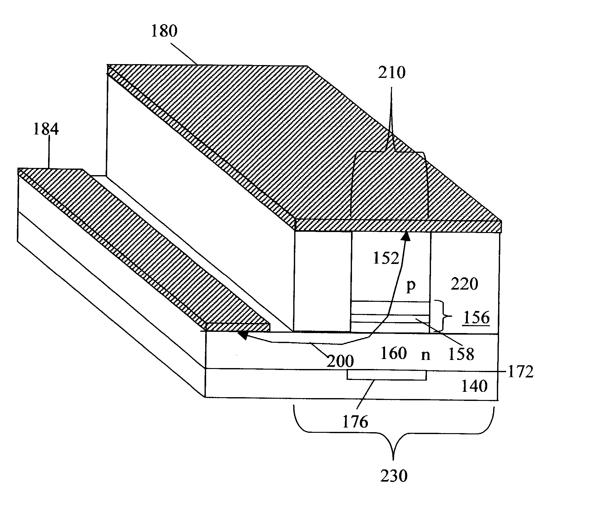
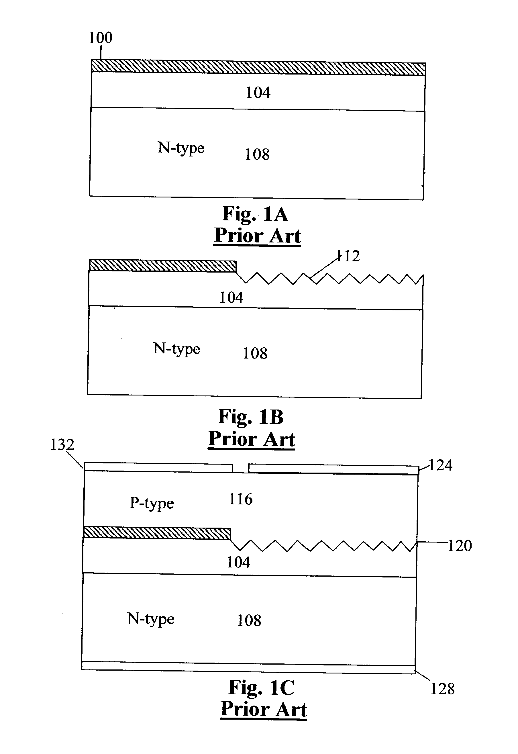
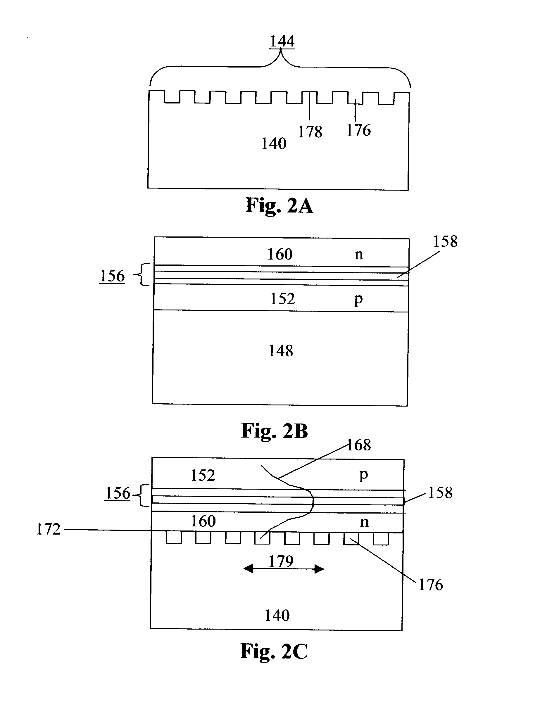
[0121] FIGS. 2A-C, 3 illustrate how a grating is incorporated at a wafer bonded interface in a DFB laser in accordance with the present invention. The discussion which follows could also apply to a grating based filter instead of a laser. Throughout this specification, the term "wafer bonding," is assumed to refer to the joining of two semiconductor surfaces through the application of heat and / or pressure, and with or without the use of interfacial adhesive layers. The two semiconductors may or may not differ in composition or lattice constant. Similarly, the term "wafer bonded interface," is assumed to comprise interfacial material if such material is employed, and the chemical bonds at that interface regardless of their nature. Additionally, "wafer bonded interfaces" or "bonded surfaces" implicitly exclude interfaces between grown epitaxial layers, between grown layers and substrates, or the surfaces between atomic planes in a continuous crystal.

[0122] In FIG. 2A, a grating 144 co...


PUM


Abstract

A semiconductor opto-electronic device according to the present invention has a grating disposed at an electrically passive wafer bonded interface. The device has p and n contacts, and current path between the contacts that does not traverse the wafer bonded interface. The absence of current injection across defective interfaces leads to a device with improved reliability relative to prior art regrowth approaches. The present invention can be combined with vertical and lateral wafer bonding to create grating-based devices with an active/passive transition, such as tunable lasers.

Description

BACKGROUND--CROSS-REFERENCES TO RELATED APPLICATIONS[0001] This application is entitled to the benefit of Provisional Patent Application Serial No. 60 / 362300, filed Mar. 6, 2002. Additionally, the specification references my co-pending U.S Patent Application entitled "Multiple Epitaxial Region Wafers with Optical Connectivity," filed by Vijaysekhar Jayaraman Jan. 15, 2003.BACKGROUND--FIELD OF THE INVENTION[0002] This invention relates generally to single-mode lasers, distributed bragg reflector lasers, distributed feedback lasers, tunable lasers, tunable filters and wafer bonding.BACKGROUND--DESCRIPTION OF PRIOR ART[0003] Semiconductor opto-electronic devices employing gratings include distributed bragg reflector (DBR) lasers, distributed feedback (DFB) lasers, sampled grating DBR (SGDBR) lasers, and grating assisted co-directional coupler lasers (GACC). Each of these laser structures can also function as a filter with slight modifications. These lasers and filters are widely employ...

Claims


Application Information

Patent Timeline
Patent Type & Authority Applications(United States)
IPC IPC(8): H01S5/12H01S5/125
CPCH01S5/12H01S2301/176H01S5/22H01S5/125
Inventor JAYARAMAN, VIJAYSEKHAR
Owner JAYARAMAN VIJAYSEKHAR
Why Eureka
Try Eureka