Semiconductor memory device having improved replacement efficiency of defective word lines by redundancy word lines

a memory device and semiconductor technology, applied in the field of semiconductor memory devices, can solve the problems of significant reduced redundancy efficiency, and increased redundancy word lines, and achieve the effect of increasing the size of semiconductor memory chips, reducing redundancy efficiency, and increasing the number of redundancy word lines

Inactive Publication Date: 2004-02-05
SAMSUNG ELECTRONICS CO LTD
View PDF4 Cites 64 Cited by
  • Summary
  • Abstract
  • Description
  • Claims
  • Application Information

AI Technical Summary

Problems solved by technology

However, if the number of banks is increased in a redundancy circuit, which is used to replace a defective memory cell with an operational memory cell, redundancy efficiency is reduced as a result of the increase in the number of banks.
The significant number of redundancy word lines necessarily increases the size of a semiconductor memory chip.

Method used


Image

  • Semiconductor memory device having improved replacement efficiency of defective word lines by redundancy word lines
  • Semiconductor memory device having improved replacement efficiency of defective word lines by redundancy word lines
  • Semiconductor memory device having improved replacement efficiency of defective word lines by redundancy word lines

Examples


Embodiment Construction

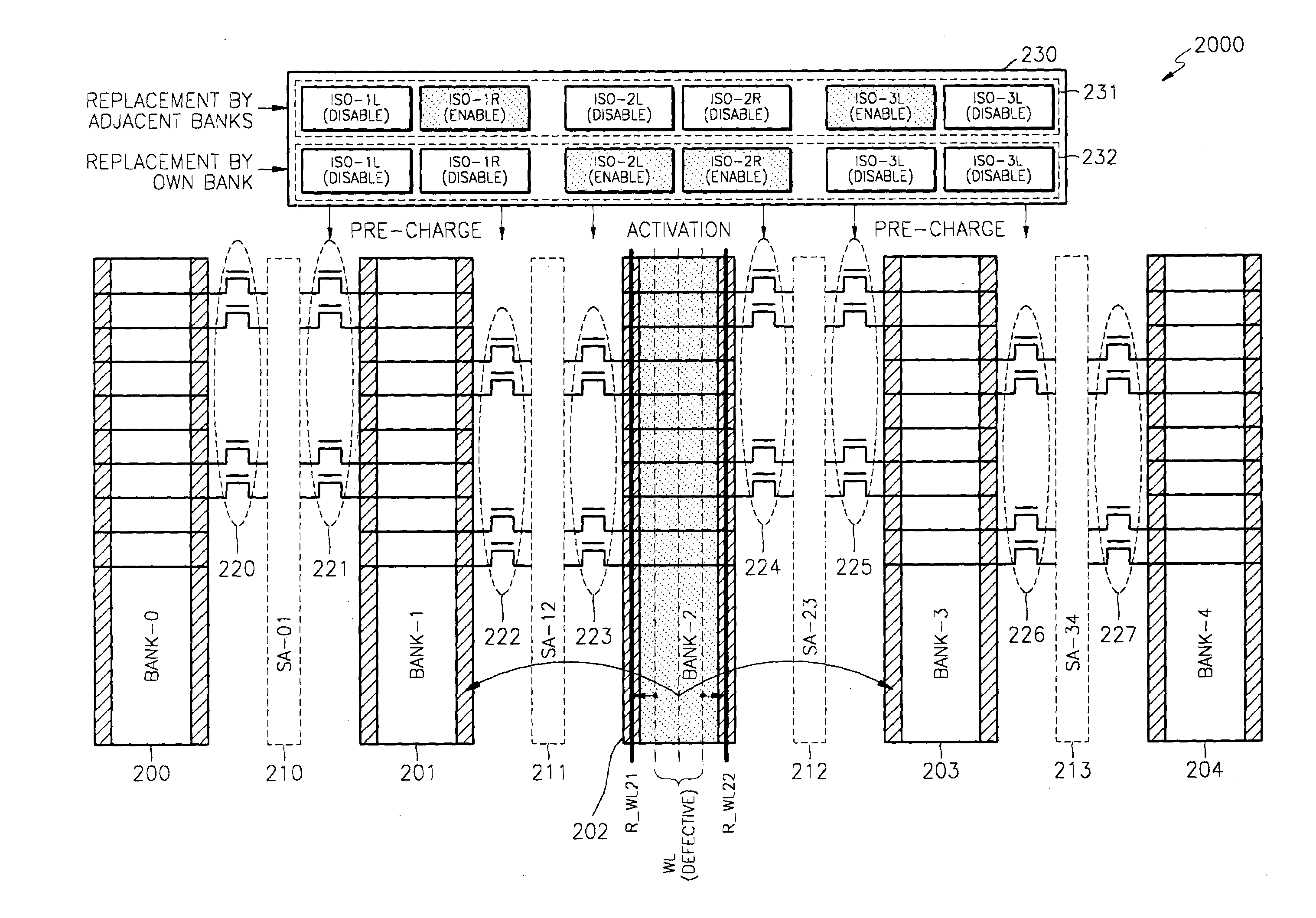
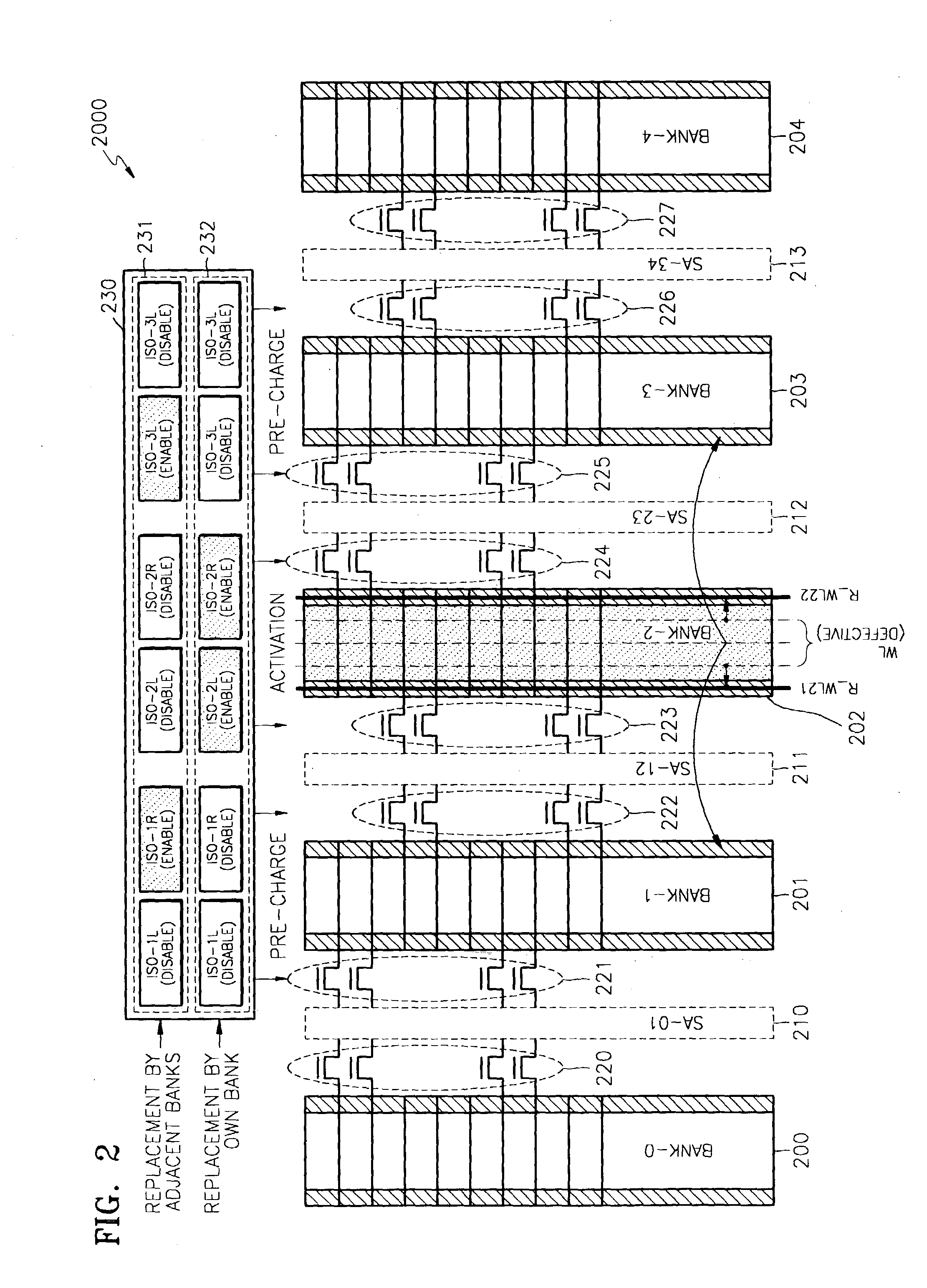
[0033] The present invention will be described more fully hereinafter with reference to the accompanying drawings in which exemplary embodiments of the invention are shown. Hereinafter, the present invention will be described in detail by describing exemplary embodiments of the invention with reference to the accompanying drawings. Like reference numerals refer to like elements throughout the drawings. The exemplary embodiments described herein are not considered as limiting the present invention.

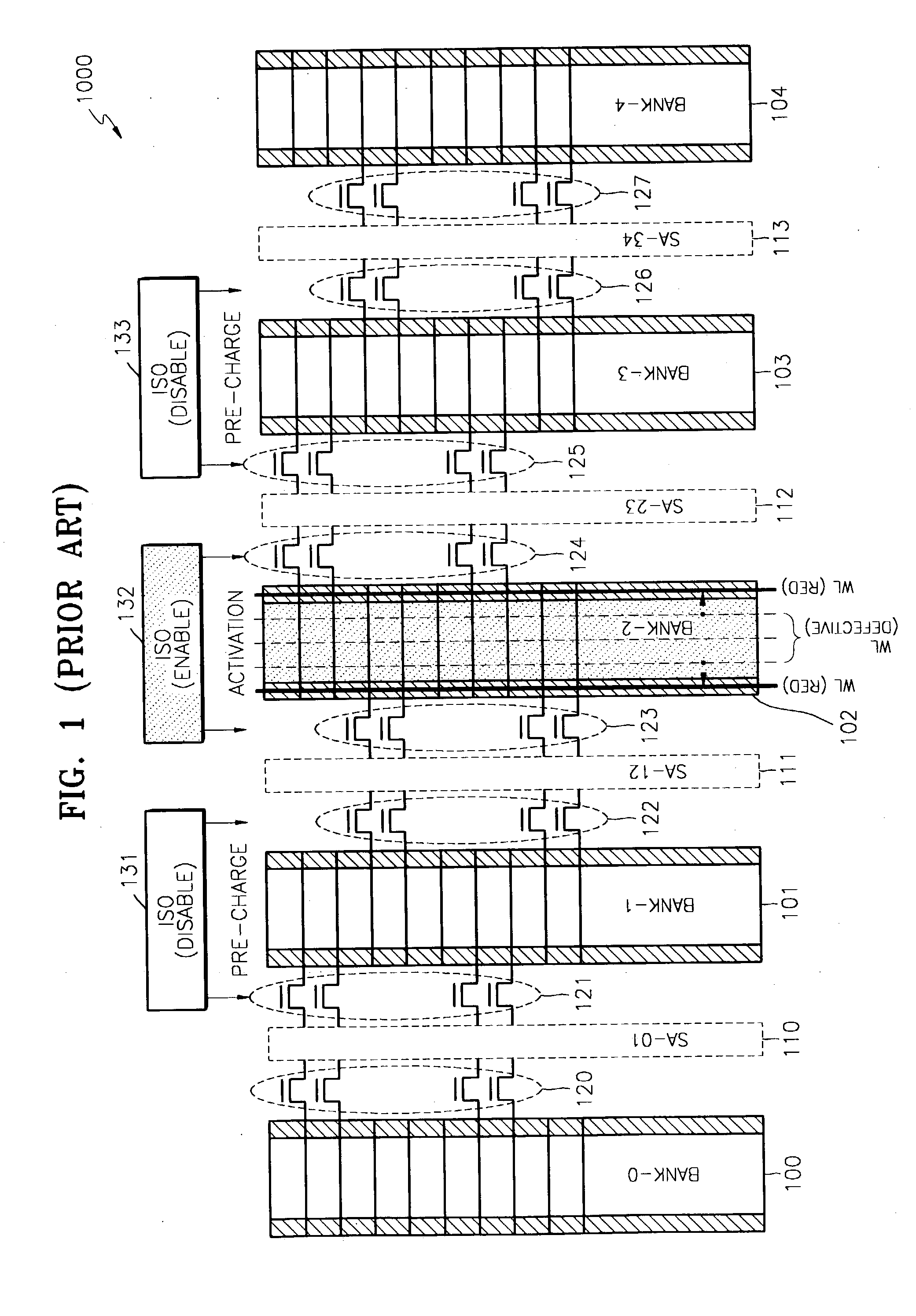
[0034] FIG. 2 illustrates an exemplary embodiment of a semiconductor memory device 2000 having a plurality of banks according to the present invention. The semiconductor memory device 2000 of FIG. 2 includes a plurality of banks 200, 201, 202, 203, and 204, a plurality of sense amplifiers 210, 211, 212, and 213, a plurality of switching circuits 220, 221, 222, 223, 224, 225, 226, and 227, and a control signal generator 230. The exemplary embodiment and the present invention are not limited ...


PUM


Abstract

A semiconductor memory device that efficiently replaces defective word lines by redundancy word lines. The semiconductor memory device includes a plurality of banks, each bank having a plurality of normal word lines and a plurality of redundancy word lines. A defective word line can be replaced by the redundancy word lines when defects occur in the normal word lines. When word line defects occur, redundancy word lines banks adjacent to the bank having the defective work line may be used.

Description

[0001] This application claims the priority of Korean Patent Application No. 2002-45892, filed Aug. 2, 2002, in the Korean Intellectual Property Office, the contents of which are incorporated herein in its entirety by reference.[0002] 1. Field of the Invention[0003] The present invention generally relates to a semiconductor memory device, and more particularly, to a semiconductor memory device having improved replacement efficiency of defective word lines by redundancy word lines in a semiconductor memory device having a plurality of banks.[0004] 2. Description of the Related Art[0005] In semiconductor memory devices, in particular, in Dynamic Random Acess Memories (DRAMs), the concept of a bank is introduced to increase the efficiency of data access time, which is known as an access time tAC. A bank is one or a plurality of DRAM blocks sharing timing control signals. Memories in a bank share a data bus, an address, and a control signal line. However, each bank is an independent chi...

Claims


Application Information

Patent Timeline
Patent Type & Authority Applications(United States)
IPC IPC(8): G11C29/00
CPCG11C29/808G11C29/00
Inventor LEE, HI-CHOON
Owner SAMSUNG ELECTRONICS CO LTD
Why Eureka
Try Eureka