Repair method for defects in data lines and flat panel display incorporating the same

Active Publication Date: 2004-09-02
AU OPTRONICS CORP
View PDF2 Cites 57 Cited by
  • Summary
  • Abstract
  • Description
  • Claims
  • Application Information

AI Technical Summary

Problems solved by technology

However, the wiring patterns may easily disconnect if the regions they pass are not smooth or during heat treatments or etching processes, resulting in open or short circuits.
Fabricating difficulties are also increased, causing higher likelihood of broken wiring patterns.
Particularly, as the number of data lines 16 increases, the number of intersecting p

Method used


Image

  • Repair method for defects in data lines and flat panel display incorporating the same
  • Repair method for defects in data lines and flat panel display incorporating the same
  • Repair method for defects in data lines and flat panel display incorporating the same

Examples


second embodiment

[0055] FIG. 5 is a top view of the pixel structure allowing repair of data line defects. FIG. 6A is a cross section taken along cut line VI-VI of FIG. 5 before repair, and FIG. 6B is a cross section taken along cut line VI-VI of FIG. 5 after repair.

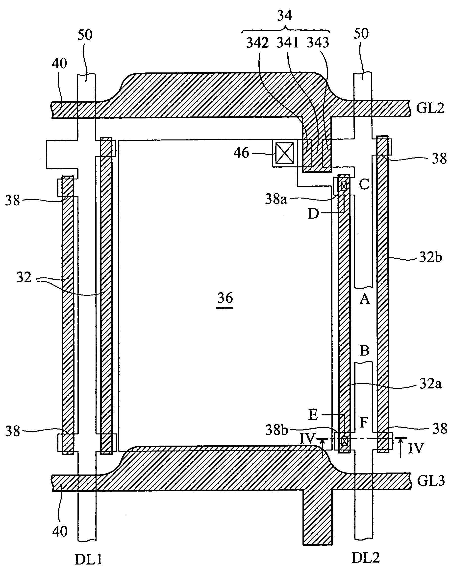
[0056] In this embodiment, the fabrication process of the active matrix substrate is substantially the same as that of the first embodiment, with the difference being the location of the backup wires 38. In this embodiment, the backup wires 38, the shielding metal lines 32, the gate electrode 341 and the gate lines 40 are fabricated at the same time, and formed from M1. The data lines 50 are formed from M2. The backup wires 38 are the protruding portions of the shielding metal lines 32.

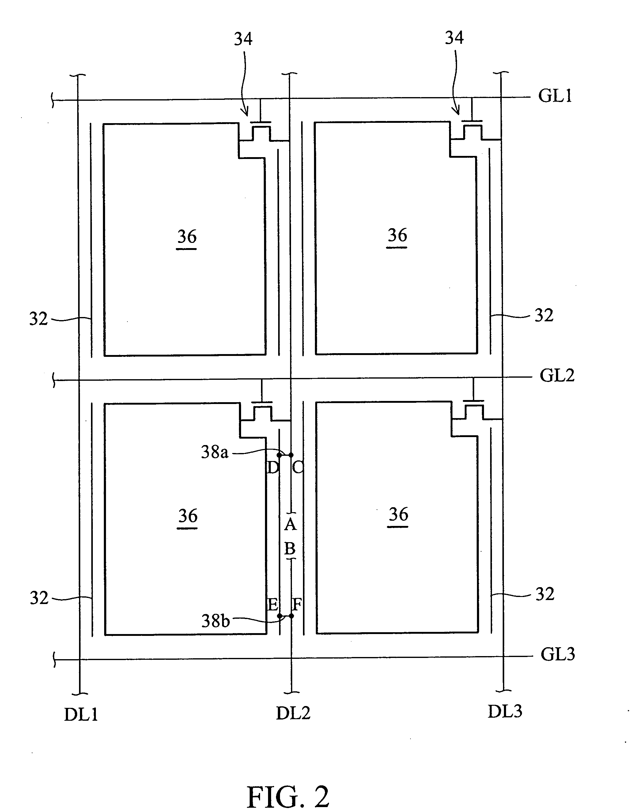
[0057] For clear description, the shielding metal lines 32 adjacent to the defect in the data line DL.sub.2 are referred to as 32a and 32b, and the protruding portions 38 for repair are referred to as 38a and 38b.

[0058] In order to ensure the fabrication qu...

third embodiment

[0059] FIG. 7 is a top view of the pixel structure allowing repair of data line defects. FIG. 8A is a cross section taken along cut line VIII-VIII of FIG. 7 before repair, and FIG. 8B is a cross section taken along cut line VIII-VIII of FIG. 7 after repair.

[0060] In this embodiment, the fabrication process of the active matrix substrate is substantially the same as that of the first embodiment, with the difference being the locations of the backup wires 38 and the shielding metal lines 32. In this embodiment, the backup wires 38, the gate electrode 341 and the gate lines 40 are fabricated at the same time, and formed from M1. The shielding metal lines 32 and the data lines 50 are fabricated at the same time, and formed from M2. The backup wires 38 and the shielding metal lines 32 are floating before repair.

[0061] For clear description, the shielding metal lines 32 adjacent to the defect in the data line DL.sub.2 are referred to as 32a and 32b, and the protruding portions 38 for repa...

fourth embodiment

[0063] FIG. 9 is a top view of the pixel structure allowing repair of data line defects. FIG. 10A is a cross section taken along cut line X-X of FIG. 9 before repair, and FIG. 10B is a cross section taken along cut line X-X of FIG. 9 after repair.

[0064] As shown in FIGS. 9 and 10, a first metal layer (M1) is formed on a substrate 30, and patterned to form a drain electrode 342, a source electrode 343, two data lines 50 and backup wires 38. An insulating layer 42, at least one semiconductor layer (not shown) and a second metal layer (M2) are sequentially formed on the substrate 30 with the drain electrode 342, the source electrode 343, the data lines 50 and the backup wires 38 thereon. After defining the second metal layer (M2), two gate lines 40, a gate electrode 341 of the TFT structure 34, and shielding metal lines 32 are formed. The shielding metal lines 32 are disposed between the pixel electrode 36 and the data lines 50 to obstruct the light in the periphery of the pixel electr...


PUM


Abstract

A method of repairing data line defects and flat panel display incorporating the same. The shielding metal lines are disposed beside the data lines and the backup wires are across the adjacent data lines/shielding metal lines to repair disconnection defects in data lines. If several defects occur in the same data line, each defect can be repaired by laser fusing using the adjacent, suitable shielding metal line and the corresponding backup wires to detour around the defect to create an electrical loop. The flat panel display further comprises the shielding metal lines disposed beside the gate lines and the backup wires across the adjacent gate lines/shielding metal lines to repair disconnection defects in gate lines.

Description

[0001] 1. Field of the Invention[0002] The present invention relates in general to a method for repairing conducting line defects. In particular, the present invention relates to a method for repairing data line defects and gate line defects in a flat panel display (FPD).[0003] 2. Description of the Related Art[0004] Liquid crystal displays (LCDs) are a well-known form of flat panel displays with advantages of low power consumption, light weight, thin profile, and low driving voltage. The liquid crystal molecules change orientation when an electronic field is applied. In the display region of the LCD, an array of pixel regions is patterned by horizontally extending gate lines and vertically extending data lines. Each pixel region has a thin film transistor (TFT) and a pixel electrode. The TFT serves as a switching device.[0005] As described above, the TFT array substrate has wiring patterns such as the gate lines and data lines, that supply image signals to drive the pixel electrode...

Claims


Application Information

Patent Timeline
IPC IPC(8): G02F1/1362
CPCG02F1/136259G02F2001/136263G02F2001/136218G02F1/136218G02F1/136263
Inventor LEE, JU-LONGLIN, YI-HSIANG
Owner AU OPTRONICS CORP
Why Eureka
Try Eureka