

Color signal compensation
a color signal and compensation technology, applied in the field of color signal compensation, can solve problems such as misalignment of read imag
- Summary
- Abstract
- Description
- Claims
- Application Information
AI Technical Summary
Problems solved by technology
Method used
Image

Examples
first embodiment
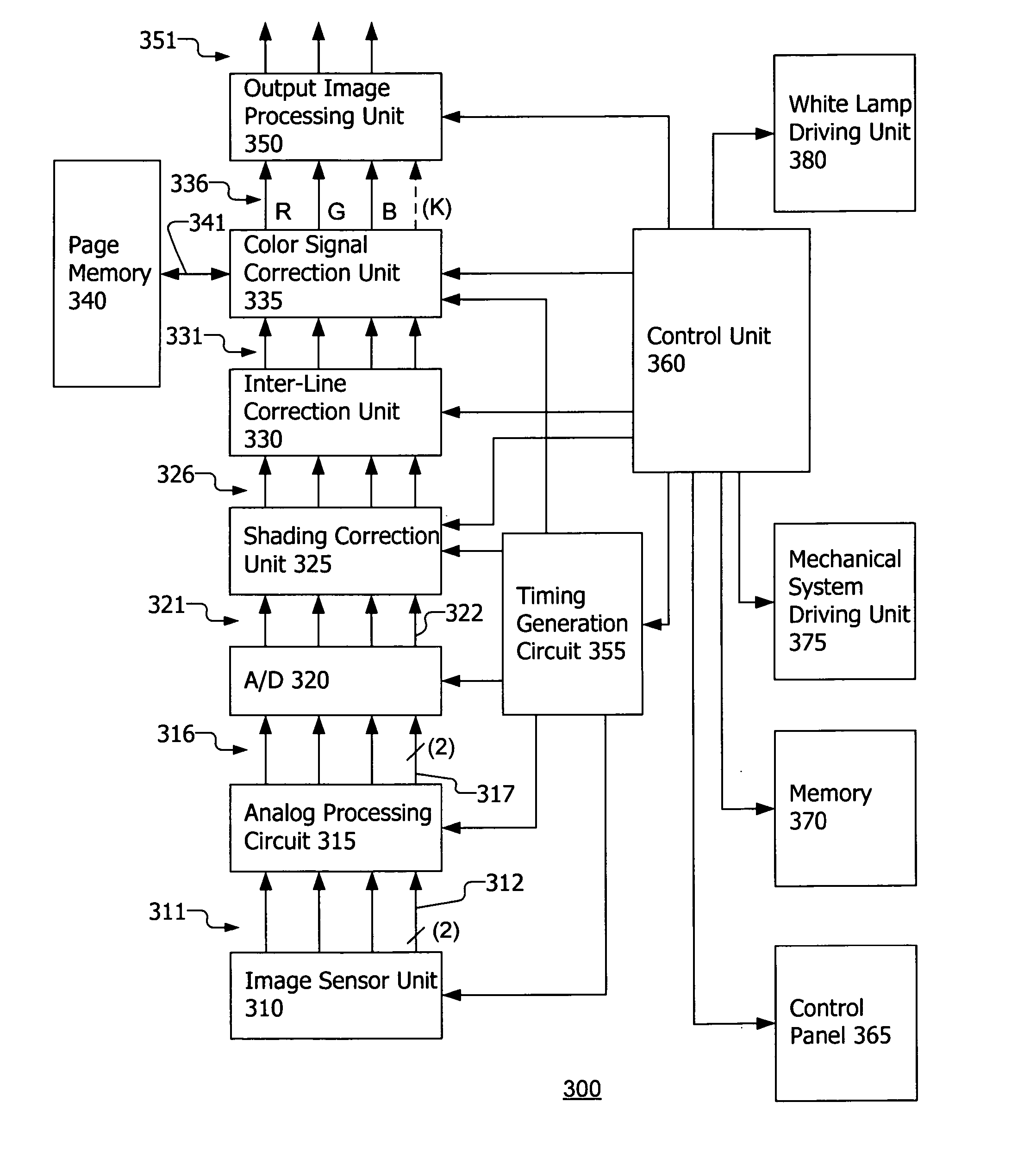
[0117] Color filters may damp the amount of light received by the color arrays. In the image sensor unit 310 of the first embodiment, the light receiving area of the photodiodes of the color arrays 2R, 2G, 2B is made wider than the light receiving area of the photodiodes of the monochrome array 2B / W. As a result, despite the damped light, good resolution may be obtained. Despite the increased width, the image sensor unit 310 is simple and compact. As a result, a decrease in cost can be obtained.
[0118] By including the monochrome photodiode array 2B / W, image quality in monochrome mode is also good.
[0119] Furthermore, the light receiving area of each color photodiode is wide, so that even if the process is performed at a speed in the sub-scanning direction 260 in color mode which is equal to the speed in the sub-scanning direction 260 in monochrome mode, the reduction in the color image quality can be minimized. This matter (single speed) means that the moving mechanism in the sub-sca...
second embodiment
[0122] (B) Second Embodiment
[0123] Next, the second embodiment of the image sensor unit and image reading apparatus of the present invention will be explained briefly with reference to the accompanying drawings. The image sensor unit and image reading apparatus of the second embodiment will be explained hereunder centering on the differences from those of the first embodiment.
[0124] Referring now to FIG. 11, there is shown a block diagram of an image sensor unit 1100 of the second embodiment. The image sensor unit 1100 has the same and corresponding parts as those of the image sensor unit 400 of the first embodiment shown in FIG. 4, so the same and corresponding reference numbers are assigned. The position of the image sensor unit 1100 to the whole image reading apparatus is shown in FIG. 3 in the same way as with the image sensor unit 400 of the first embodiment.
[0125] In the second embodiment, the relationship between the light receiving surface of the photodiodes of the color pho...
third embodiment
[0145] (C) Third Embodiment
[0146] Referring now to FIG. 14, there is shown a block diagram of an image sensor unit 1400 of a third embodiment. In FIG. 14, the same and corresponding numerals are assigned to the same and corresponding parts as those of the image sensor unit 400 of the first embodiment.
[0147] The position of the image sensor unit 1400 to the whole image reading apparatus is the position shown in FIG. 3 in the same way as with the image sensor unit 400 of the first embodiment.
[0148] In the image sensor unit 1400, the relationship between the light receiving surface of each photodiode of the photodiode arrays 2R, 2G, 2B for the three primary colors R, G, B and the light receiving surface of each photodiode of the monochrome photodiode array 2B / W may be the same as that of the first embodiment.
[0149] The difference of the image sensor unit 1400 from that of the first embodiment is a constitution for outputting the stored charge of the monochrome photodiode array 2B / W. In...
PUM
 Abstract
Description
Claims
Application Information