Electromechanical memory array using nanotube ribbons and method for making same

a technology of nanotube ribbons and memory arrays, applied in nanoelectromechanical switches, relays, instruments, etc., can solve the problems of long write cycles (ms), low relative speed in comparison to dram or sram, and relatively low cost of roms,

Inactive Publication Date: 2004-10-28
NANTERO
View PDF99 Cites 111 Cited by
  • Summary
  • Abstract
  • Description
  • Claims
  • Application Information

AI Technical Summary

Problems solved by technology

ROM is relatively low cost but cannot be rewritten.
EEPROM (or "Flash") is inexpensive, and has low power consumption but has long write cycles (ms) and low relative speed in comparison to DRAM or SRAM.
Flash also has a finite number of read/write cycles leading to low long-term reliability.
SRAM does not need to be refreshed and is fast relative to DRAM, but has lower density and is more expensive relative to DRAM.
Both SRAM and DRAM are volatile, meaning that if power to the memory is interrupted the memory will lose the information stored in the memory cells.
Consequently, existing technologies are either non-volatile but are not randomly accessible and have low density, high cost, and limited ability to allow multiples writes with high reliability of the circuit's function, or they are volatile and complicate system design or have low density.
A different memory cell based upon magnetic

Method used


Image

  • Electromechanical memory array using nanotube ribbons and method for making same
  • Electromechanical memory array using nanotube ribbons and method for making same
  • Electromechanical memory array using nanotube ribbons and method for making same

Examples


Embodiment Construction

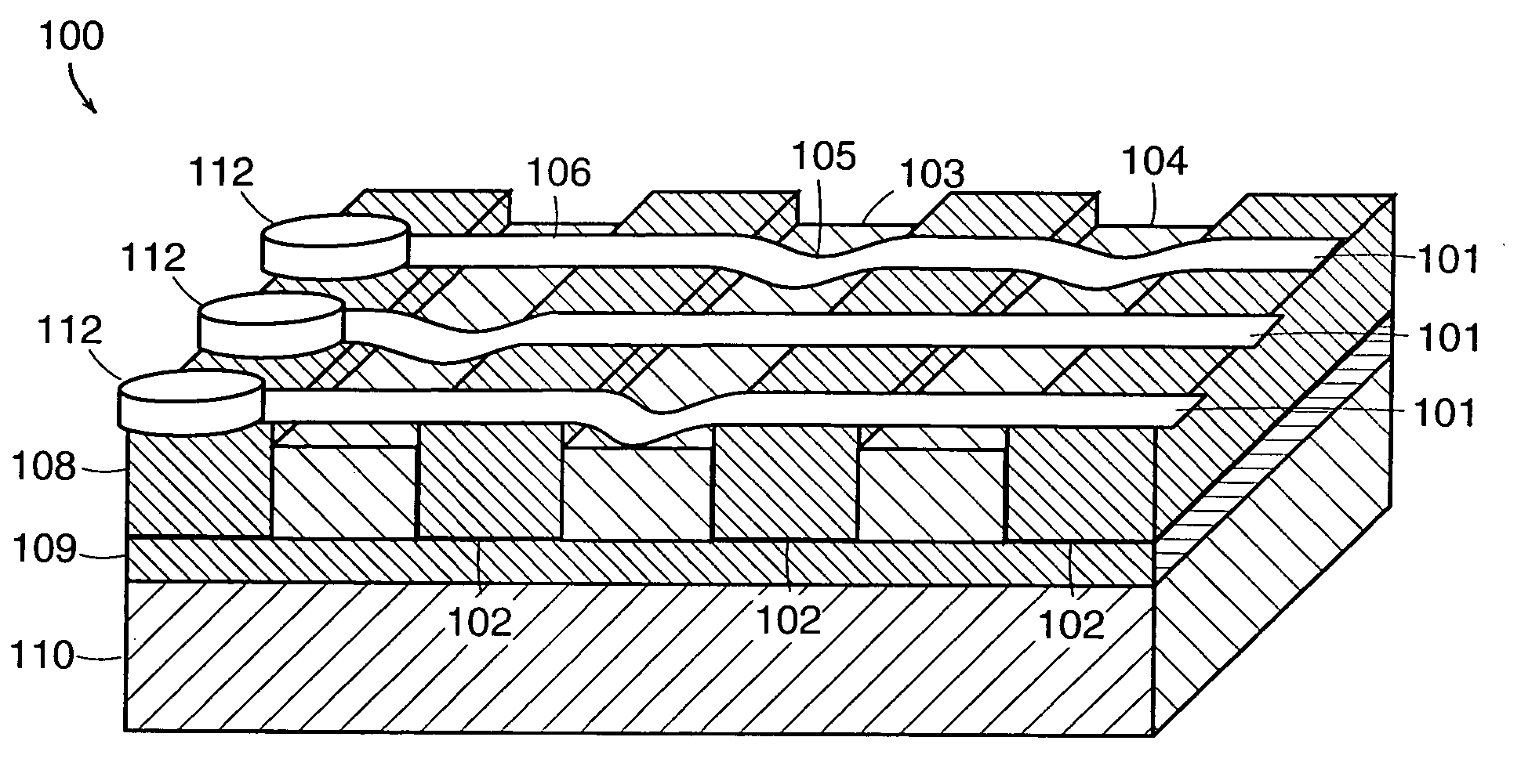
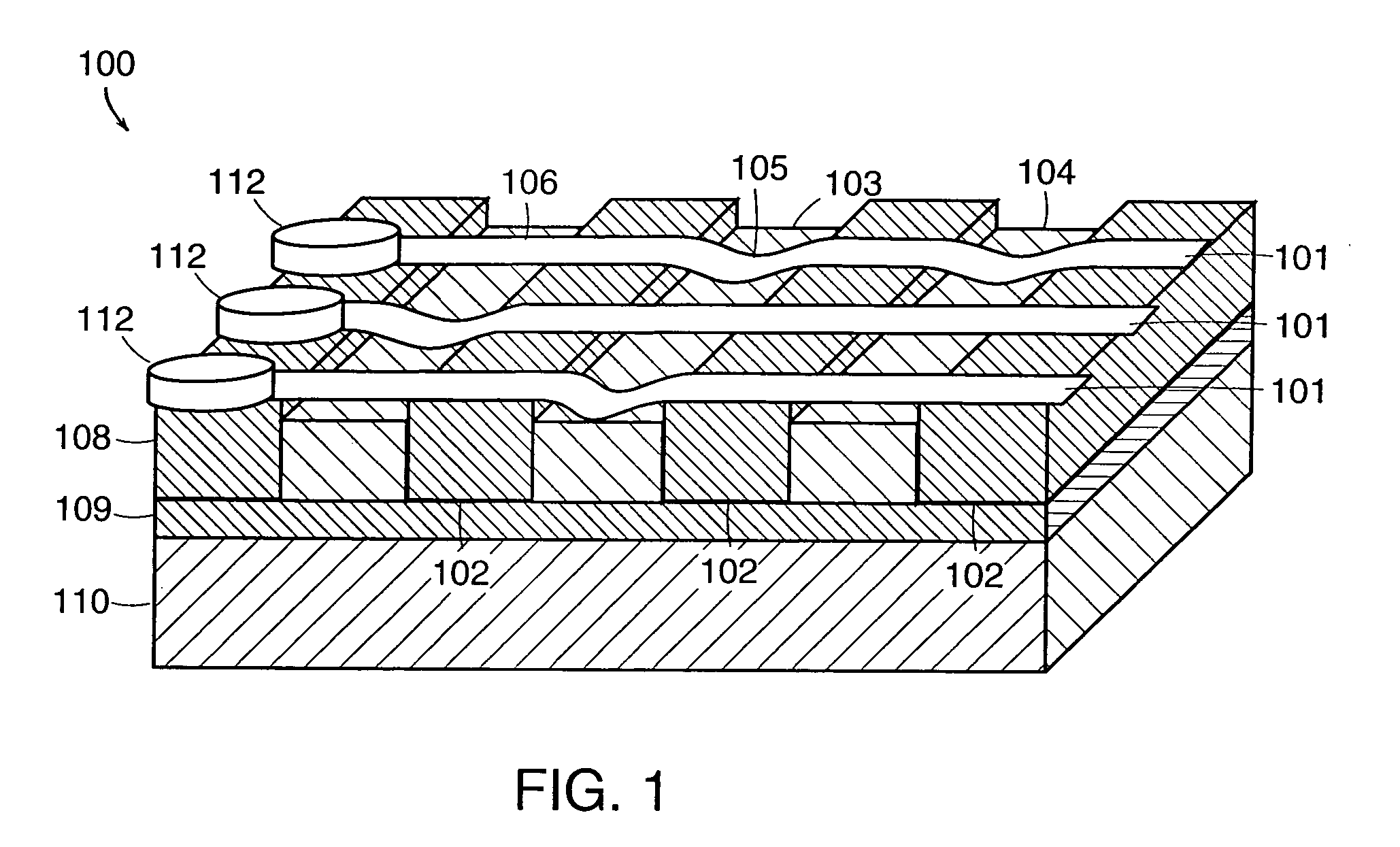
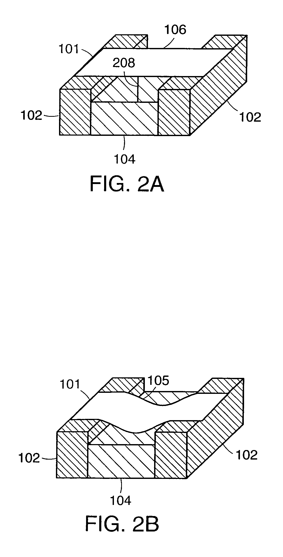
[0097] Besides carbon nanotubes other materials with electronic and mechanical properties suitable for electromechanical switching could be envisioned. These materials would have properties similar to carbon nanotubes but with different and likely reduced tensile strength. The tensile strain and adhesion energies of the material must fall within a range to allow bistability of the junction and electromechanical switching properties to exist within acceptable tolerances.

[0098] For the purpose of integrating CMOS logic for addressing two approaches can be envisioned. In the first embodiment the nanotube array will be integrated before metallization but after ion implantation and planarization of the CMOS logic devices. A second method involves growth of the nanotube arrays before fabrication of the CMOS devices involving ion implementation and high temperature annealing steps. Upon completion of these steps the final metallization of both the nanotube ribbons and the CMOS devices will...


PUM


Abstract

Electromechanical circuits, such as memory cells, and methods for making same are disclosed. The circuits include a structure having electrically conductive traces and supports extending from a surface of the substrate, and nanotube ribbons suspended by the supports that cross the electrically conductive traces, wherein each ribbon comprises one or more nanotubes. The electromechanical circuit elements are made by providing a structure having electrically conductive traces and supports, in which the supports extend from a surface of the substrate. A layer of nanotubes is provided over the supports, and portions of the layer of nanotubes are selectively removed to form ribbons of nanotubes that cross the electrically conductive traces. Each ribbon includes one or more nanotubes.

Description

[0001] This application is a divisional and claims priority under 35 U.S.C. .sctn.121 to U.S. patent application Ser. No. 09 / 915,093, filed on Jul. 25, 2001, entitled ELECTROMECHANICAL MEMORY ARRAY USING NANOTUBE RIBBONS AND METHOD FOR MAKING SAME.[0002] The following applications are incorporated by reference in their entirety:[0003] U.S. patent application Ser. No. 09 / 915,095, filed on Jul. 25, 2001, now U.S. Pat. No. 6,574,130, entitled HYBRID CIRCUIT HAVING NANOTUBE ELECTROMECHANICAL MEMORY; and[0004] U.S. patent application Ser. No. 09 / 915,173, filed on Jul. 25, 2001, now U.S. Pat. No. 6,643,165, entitled ELECTROMECHANICAL MEMORY HAVING CELL SELECTION CIRCUITRY CONSTRUCTED WITH NANOTUBE TECHNOLOGY.[0005] 1. Technical Field[0006] This invention relates in general to nonvolatile memory devices for use as memory storage in an electronic device and in particular to nonvolatile memory arrays that use electromechanical elements as the individual memory cells.[0007] 2. Discussion of R...

Claims


Application Information

Patent Timeline
IPC IPC(8): B82B1/00B81B3/00B82B3/00G11C13/02G11C23/00H01H59/00H01L21/768H01L27/10H01L29/06
CPCB82Y10/00Y10T428/24893G11C23/00G11C2213/16G11C2213/81H01H1/0094H01L21/76838H01L27/10Y10S977/742Y10S977/888Y10S977/856Y10S977/943Y10S977/724Y10S977/796Y10T428/24917G11C13/025
Inventor SEGAL, BRENT M.BROCK, DARREN K.RUECKES, THOMAS
Owner NANTERO
Why Eureka
Try Eureka