Silicon-on-insulator latch-up pulse-radiation detector

a technology of latching and radiation detector, which is applied in the direction of radiation intensity measurement, instruments, x/gamma/cosmic radiation measurement, etc., can solve the problems of unsuitable design for radiation detector use, and difficulty in producing a soi radiation detector in which ionizing radiation-triggered latching can occur

Active Publication Date: 2005-01-06
TAIWAN SEMICON MFG CO LTD
View PDF11 Cites 4 Cited by
  • Summary
  • Abstract
  • Description
  • Claims
  • Application Information

AI Technical Summary

Problems solved by technology

Unfortunately, because one of the characteristics of SOI technology is the substantial reduction of latch-up, it has proven very difficult to produce an SOI radiation detector in which ionizing-radiation-triggered latch-up can occur.
Unfortunately, the bulk CMOS structure relies on a current path beneath the device isolation which is absent in SOI technology, thus making this design unsuitable for use as a radiation detector.

Method used


Image

  • Silicon-on-insulator latch-up pulse-radiation detector
  • Silicon-on-insulator latch-up pulse-radiation detector
  • Silicon-on-insulator latch-up pulse-radiation detector

Examples


Embodiment Construction

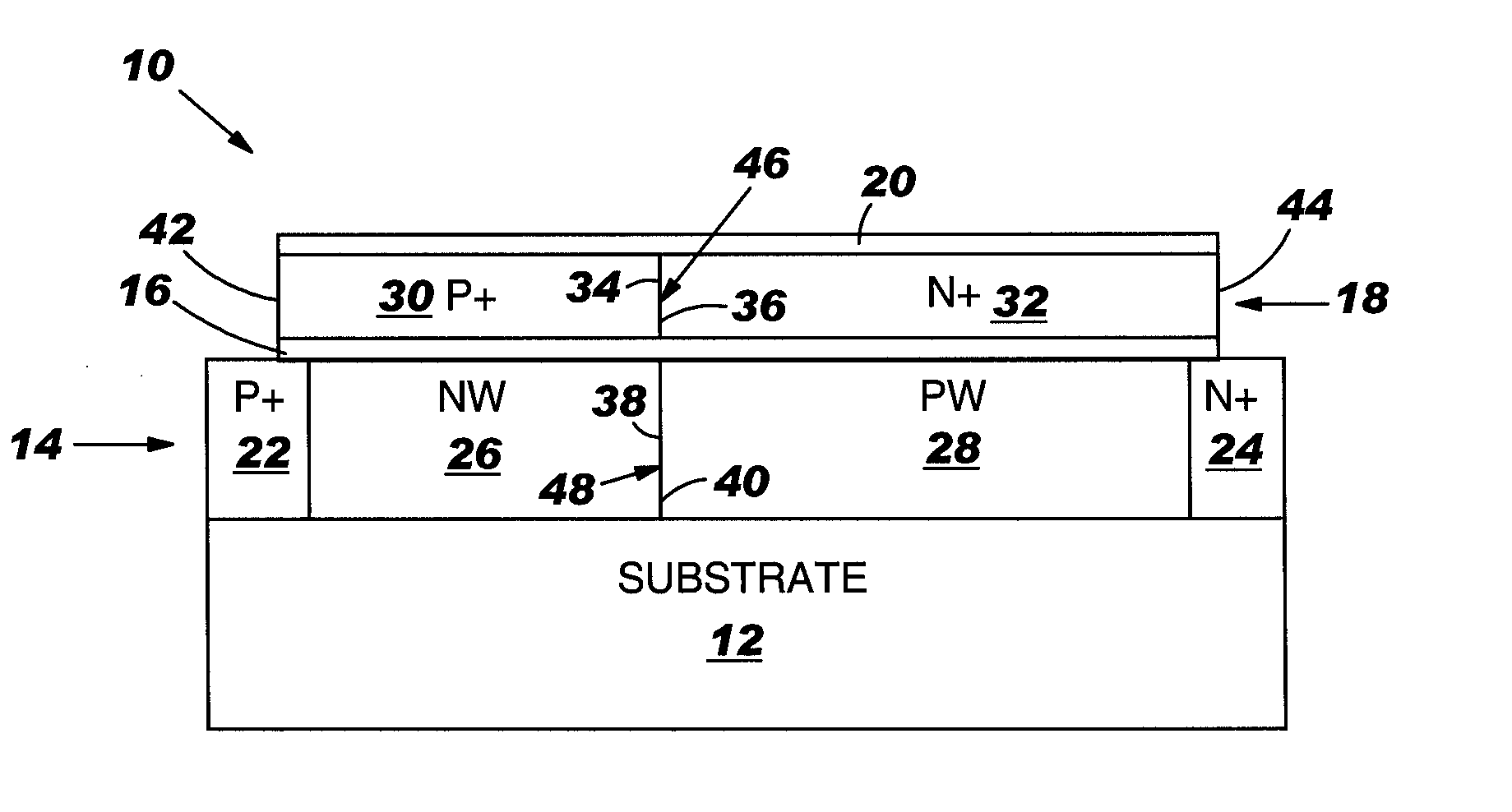
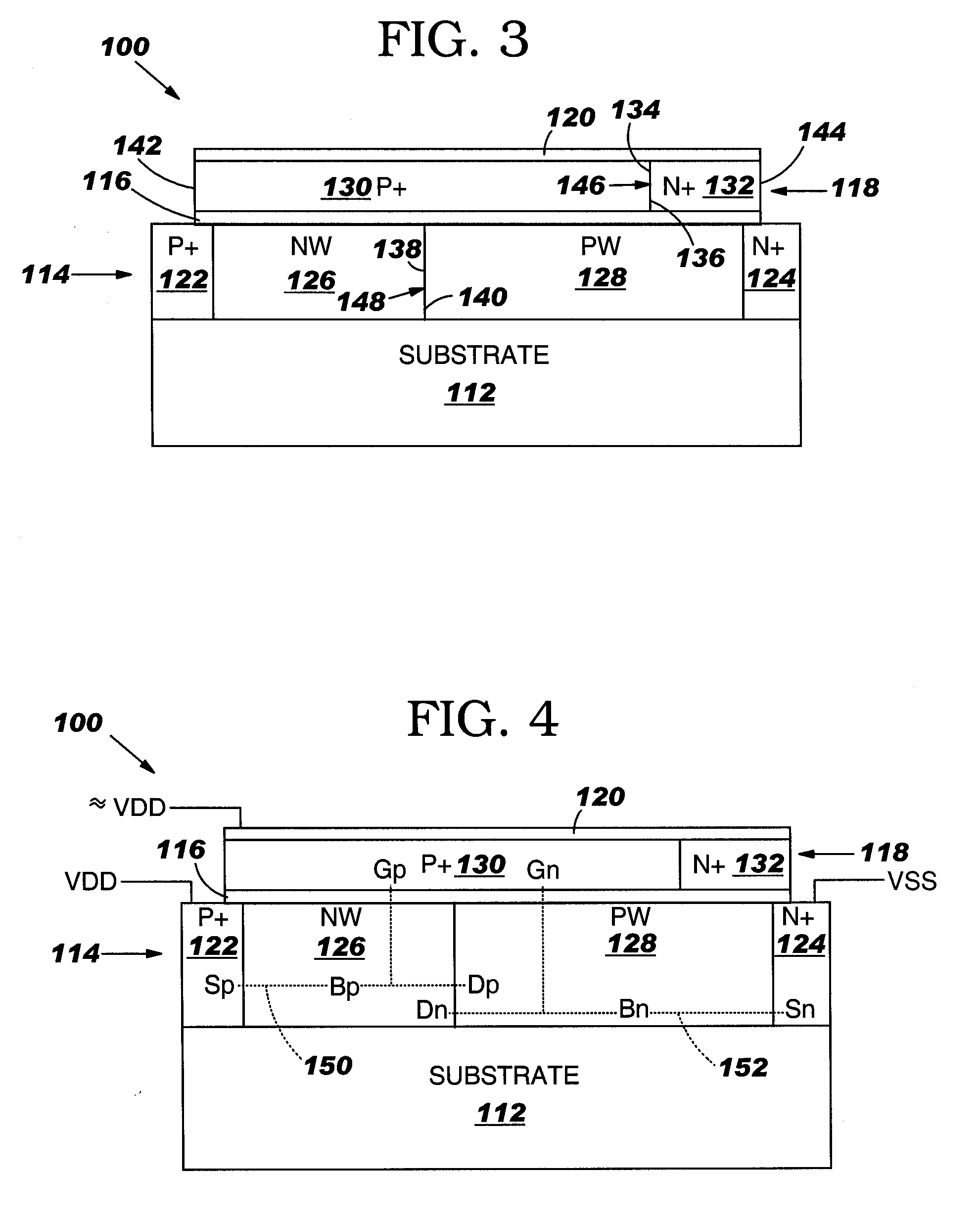
[0023] A first embodiment of an SOI radiation detector in accordance with the present invention, formed as a PNPN diode structure 100, is illustrated in FIG. 3. The PNPN diode structure 100 shown in FIG. 3 comprises an insulating substrate 112, a silicon layer 114 formed on the insulating substrate 112, a gate oxide layer 116 formed on the silicon layer 114, a gate layer 118 formed on the gate oxide layer 116, and a silicide strap 120 formed over the gate layer 118. The silicon layer 114 includes a heavily doped P+region 122, a heavily doped N+region 124, a lightly-doped N-well 126, and a lightly doped P-well 128. The gate layer 118 includes a heavily doped P+region 130 and a heavily doped N+region 132 tied together by the silicide strap 120. The PNPN diode structure 100 can be formed using conventional SOI processes known to those skilled in the art.

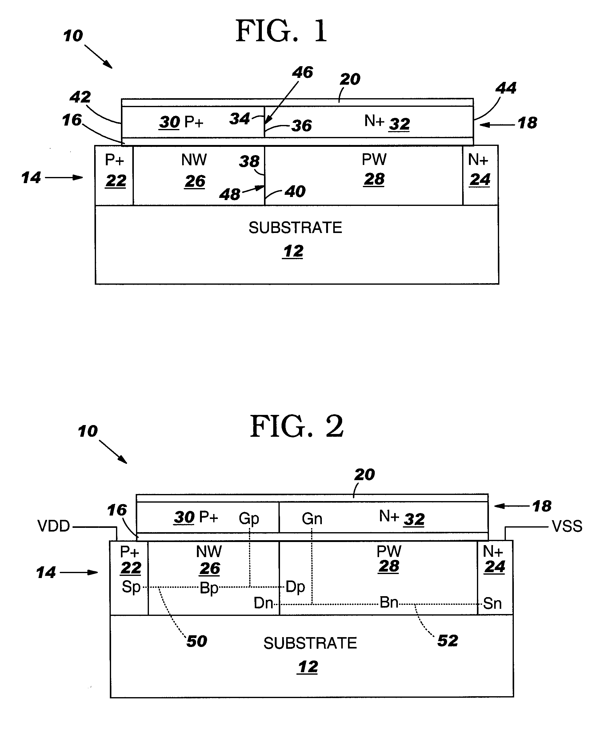
[0024] As detailed above, in the PNPN diode structure 10 shown in FIG. 1, the interface 46 between the P+region 30 and the N+region 3...


PUM


Abstract

A radiation detector formed using silicon-on-insulator technology. The radiation detector includes a silicon layer formed on an insulating substrate, wherein the silicon layer includes a PNPN structure, and a gate layer formed over the PNPN structure, wherein the gate layer includes a PN gate. Latch-up occurs in the radiation detector only in response to incident radiation.

Description

BACKGROUND OF INVENTION [0001] 1. Technical Field [0002] The present invention relates generally to integrated circuits, and more particularly, to a latch-up pulse-radiation detector formed using silicon-on-insulator (SOI) technology. [0003] 2. Related Art [0004] Silicon-on-insulator (SOI) technology, which is becoming of increasing importance in the field of integrated circuits, deals with the formation of semiconductor devices (e.g., diodes, transistors, etc.) in a relatively thin layer of semiconductor material overlaying a layer of insulating material. SOI technology offers many advantages over bulk complementary metal-oxide-semiconductor (CMOS) processes, including, for example, higher performance, higher packing density, lower power consumption, and a substantial reduction of latch-up. [0005] The cause of latch-up exists in all junction-isolated or bulk CMOS processes: parasitic PNPN paths. The resultant parasitic PNP and NPN bipolar transistors formed by such parasitic PNPN p...

Claims


Application Information

Patent Timeline
Patent Type & Authority Applications(United States)
IPC IPC(8): G01T1/24H01L27/12H01L31/111
CPCH01L31/1113H01L27/12
Inventor COTTRELL, PETER E.DENNARD, ROBERT H.NOWAK, EDWARD J.ROHRER, NORMAN J.
Owner TAIWAN SEMICON MFG CO LTD
Why Eureka
Try Eureka