Methods of cutting or forming cavities in a substrate for use in making optical films, components or wave guides

a technology of optical film and substrate, applied in the field of cutting or forming cavities in the substrate for use in making optical films, components or wave guides, can solve the problems of short useful life, high cost and expense of cutting or forming cavities of certain types of optical elements, and the difficulty of spinning tools needed to make geometric shapes such as these, so as to achieve the effect of substantially reducing the length and width of the optical substra

Inactive Publication Date: 2005-02-03
SOLID STATE OPTO
View PDF7 Cites 256 Cited by
  • Summary
  • Abstract
  • Description
  • Claims
  • Application Information

AI Technical Summary

Benefits of technology

[0005] The difficulty and cost of making optical substrates including one or more patterns of optical elements having at least two surfaces that come together to form a ridge and are quite small relative to the length and width of the optical substrates are substantially reduced by using a tool to cut or form cavities of suc

Problems solved by technology

A drawback to this method is the difficulty and expense of cutting or forming cavities of certain types of optical element shapes including particularly those having at least two surfaces that come together to form a ridge and are quite small relative to the length and width of t

Method used


Image

  • Methods of cutting or forming cavities in a substrate for use in making optical films, components or wave guides
  • Methods of cutting or forming cavities in a substrate for use in making optical films, components or wave guides
  • Methods of cutting or forming cavities in a substrate for use in making optical films, components or wave guides

Examples


Embodiment Construction

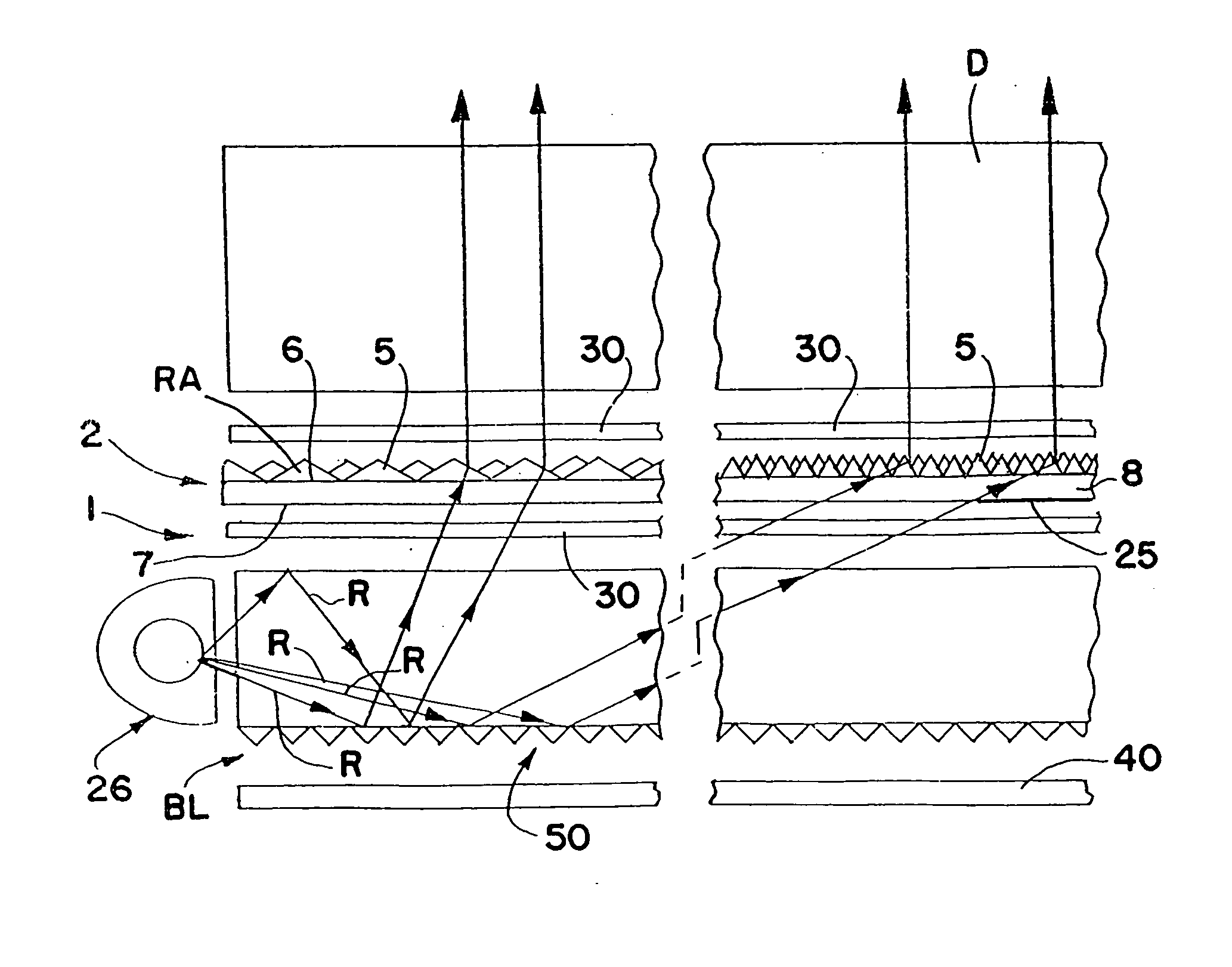
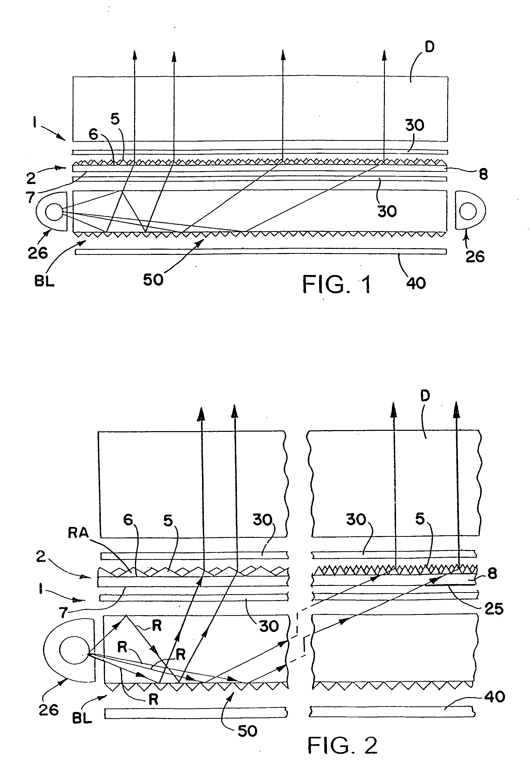
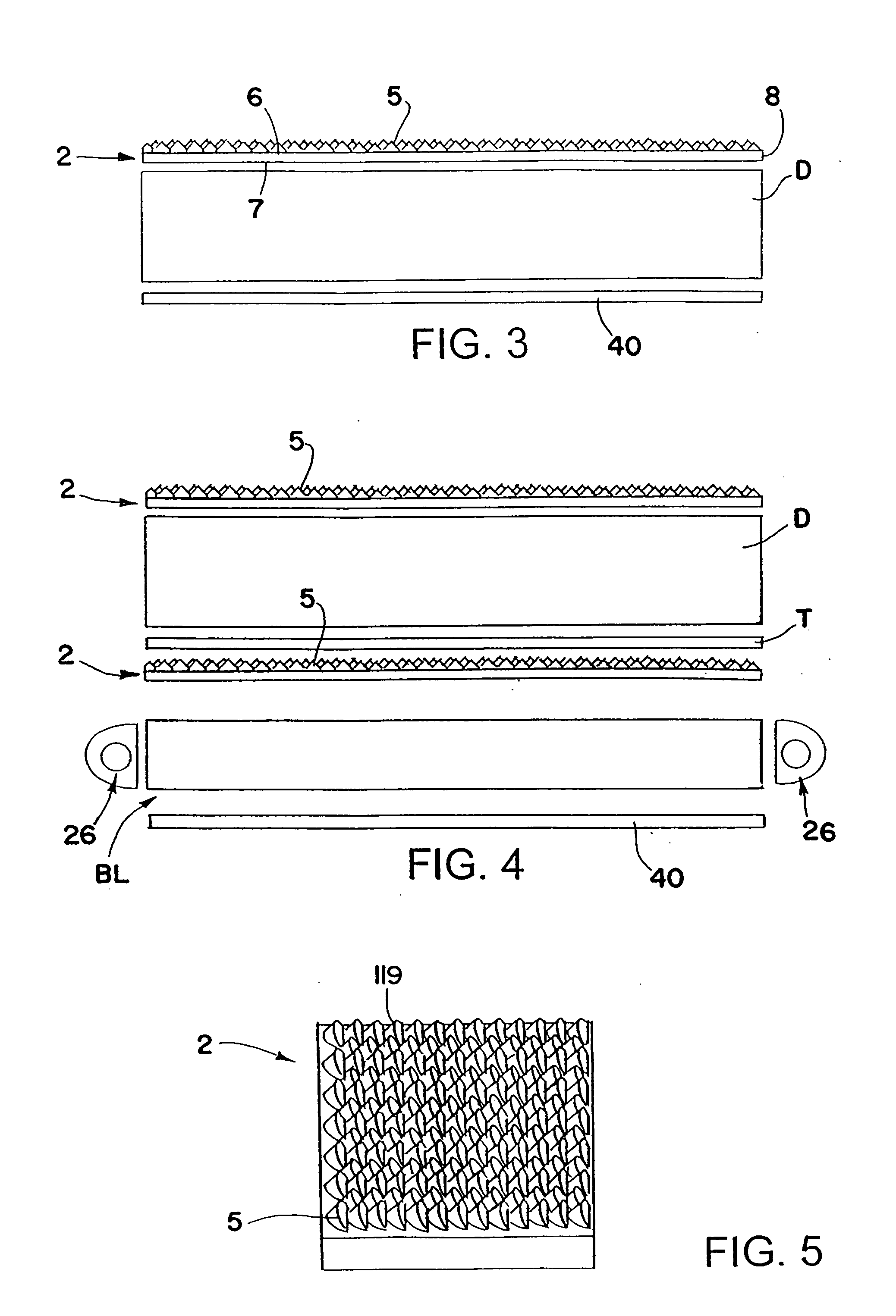
[0041]FIGS. 1 and 2 schematically show one form of light redirecting film system 1 in accordance with this invention including a light redirecting film 2 that redistributes more of the light emitted by a backlight BL or other light source toward a direction more normal to the surface of the film. Film 2 may be used to redistribute light within a desired viewing angle from almost any light source for lighting, for example, a display D such as a liquid crystal display, used in laptop computers, word processors, avionic displays, cell phones, PDAs and the like, to make the displays brighter. The liquid crystal display can be any type including a transmissive liquid crystal display as schematically shown in FIGS. 1 and 2, a reflective liquid crystal display as schematically shown in FIG. 3 and a transflective liquid crystal display as schematically shown in FIG. 4.

[0042] The reflective liquid crystal display D shown in FIG. 3 includes a back reflector 40 adjacent the back side for refl...


PUM

PropertyMeasurementUnit
Fractionaaaaaaaaaa
Angleaaaaaaaaaa
Angleaaaaaaaaaa

Abstract

The methods involve using a tool to cut or form multiple optical element shaped cavities in a surface of a substrate without rotating the tool or substrate during the cutting or forming process. At least some of the cavities are cut or formed to have at least two surfaces that come together to form a ridge and that are quite small relative to the length and width of the substrate. Thereafter the substrate is used to form optical films, components or wave guides having multiple optical elements on at least one surface corresponding to the cavities in the substrate.

Description

CROSS-REFERENCE TO RELATED APPLICATIONS [0001] This application is a continuation-in-part of U.S. patent application Ser. No. 10 / 729,113, filed Dec. 5, 2003, which is a division of U.S. patent application Ser. No. 09 / 909,318, filed Jul. 19, 2001, now U.S. Pat. No. 6,752,505, dated Jun. 22, 2004, which is a continuation-in-part of U.S. patent application Ser. No. 09 / 256,275, filed Feb. 23, 1999, now U.S. Pat. No. 6,712,481, dated Mar. 30, 2004, the entire disclosures of which are incorporated herein by reference.FIELD OF THE INVENTION [0002] This invention relates to methods of cutting or forming one or more patterns of optical element shaped cavities in a substrate for use in forming corresponding patterns of optical elements on or in optical substrates including films, components or wave guides and the like. BACKGROUND OF THE INVENTION [0003] It is generally known to provide multiple optical elements on or in one or more surfaces of optical substrates including films, components or...

Claims


Application Information

Patent Timeline
IPC IPC(8): F21V5/00F21V8/00
CPCF21V5/00G02B6/0036G02B6/0065G02B6/0053G02B6/0061G02B6/0038B29D7/00G02B6/12
Inventor PARKER, JEFFERY R.MCCOLLUM, TIMOTHY A.EZELL, ROBERT M.STARKEY, KURT R.
Owner SOLID STATE OPTO
Why Eureka
Try Eureka