Semiconductor device

a technology of semiconductor devices and semiconductors, applied in semiconductor devices, semiconductor/solid-state device details, electrical apparatus, etc., can solve the problems of increasing the device size in view, affecting the meltdown speed of the fuse, increasing the cost of the process, etc., to facilitate the meltdown of the fuse, and concentrate the heat generated.

Active Publication Date: 2005-02-10
RENESAS ELECTRONICS CORP
View PDF8 Cites 36 Cited by
  • Summary
  • Abstract
  • Description
  • Claims
  • Application Information

AI Technical Summary

Benefits of technology

[0018] As has been explained in the above, in the semiconductor device mounted with the fuse of the present invention, a portion-to-be-melted of the fuse is surrounded by the plates, so that heat to be generated in the meltdown portion of the fuse under current supply can be confined or accumulated in the vicinity of the meltdown portion o...

Problems solved by technology

The method of blowing the fuse off using the laser, however, raises several problems.
A first problem resides in that a position of disconnection of the fuse must be apart from other elements by a predetermined distance so as to avoid any possible influences of the laser-assisted disconnection of the fuse, and this increases the device size in view...

Method used


Image

  • Semiconductor device
  • Semiconductor device
  • Semiconductor device

Examples


embodiment 1

[0027] [Embodiment 1]

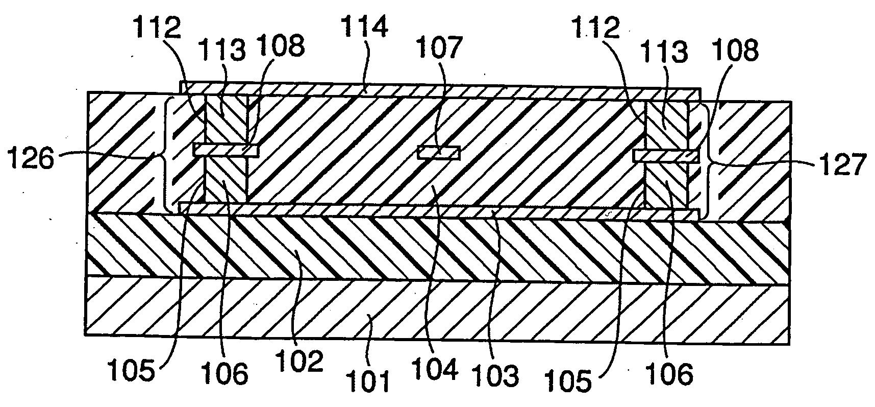
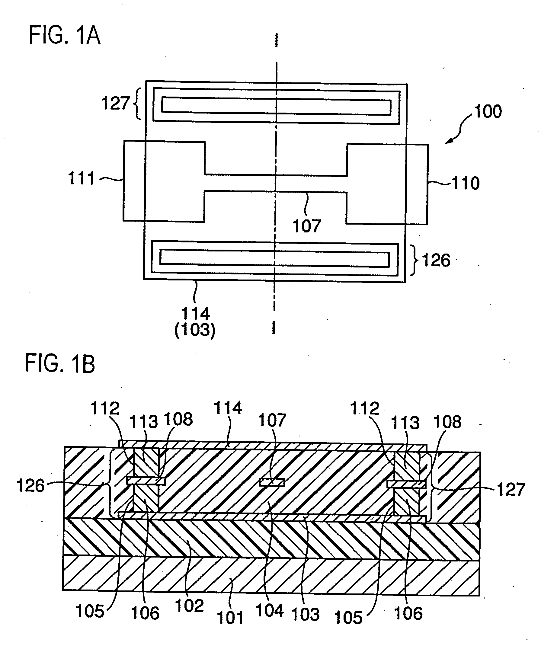
[0028] A first embodiment of the present invention will be explained referring to FIG. 1A and FIG. 1B. The first embodiment shows a case where a fuse, which is a straight-line-formed conductor, is disposed in parallel to the surface of a semiconductor substrate. FIG. 1A is a plan view of the fuse, and FIG. 1B is a sectional view taken along line I-I in FIG. 1A.

[0029] As shown in FIGS. 1A and 1B, a fuse 100 is provided in a second interlayer dielectric film 104 on a first interlayer dielectric film 102 on a semiconductor substrate 101. It is to be noted that the second interlayer dielectric film 104 is practically composed of a plurality of interlayer dielectric films although it is illustrated herein as a single layer for the simplicity of explanation. The fuse 100 is covered with a lower plate 103 and an upper plate 114, which compose a pair of parallel plates, respectively on the lower and upper portions of a fuse meltdown portion 107, and with via plugs 106,...

embodiment example 2

[0039] [Embodiment Example 2]

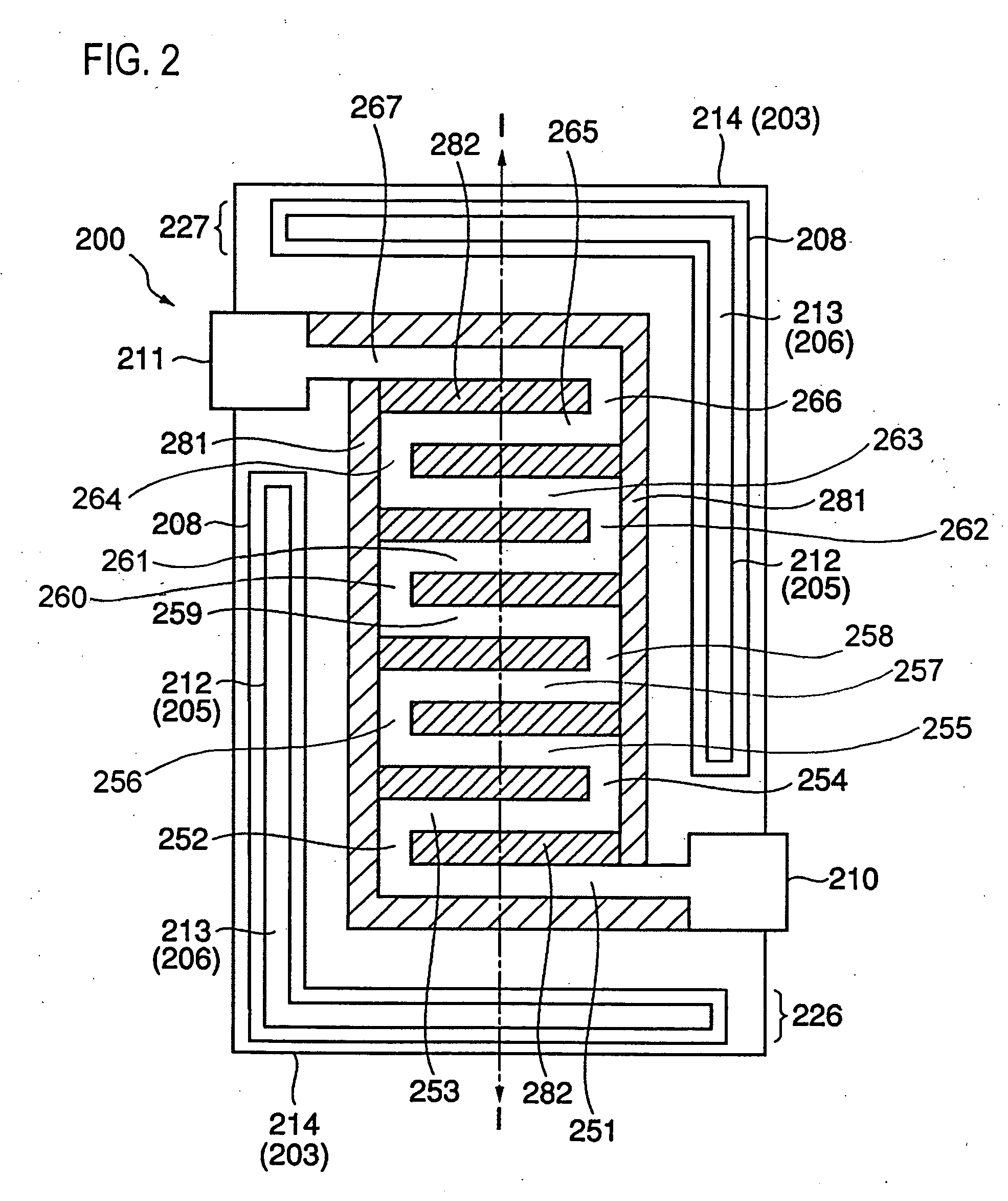
[0040] The foregoing embodiment described a case where the fuse was disposed in parallel to the surface of the semiconductor substrate. Then, a second embodiment will describe a case where the fuse is disposed normal to the surface of the semiconductor substrate referring to FIG. 4A, FIG. 4B and FIG. 5. FIG. 4A is a plan view of the fuse, FIG. 4B is a sectional view taken along line II-II in FIG. 4A, and FIG. 5 is a sectional view taken along line III-III in FIG. 4A.

[0041] As shown in FIGS. 4A and 4B, a fuse 400 is disposed in a second interlayer dielectric film 404 on a first interlayer dielectric film 402 on a semiconductor substrate 401. It is to be noted that the second interlayer dielectric film 404 is practically composed of a plurality of interlayer dielectric films although it is illustrated herein as a single layer for the simplicity of explanation. The fuse 400 is covered with a lower plate 403 and an upper plate 414 on the lower and upper sid...


PUM


Abstract

A portion-to-be-melted of a fuse is surrounded by plates, so that heat to be generated in a meltdown portion of the fuse under current supply can be confined or accumulated in the vicinity of the meltdown portion of the fuse. This makes it possible to facilitate meltdown of the fuse. The meltdown portion of the fuse in a folded form, rather than in a single here a fuse composed of a straight-line form, is more successful in readily concentrating the heat generated in the fuse under current supply into the meltdown portion, and in further facilitating the meltdown of the fuse.

Description

[0001] This application is based on Japanese patent application No. 2003-288829, the content of which is incorporated hereinto by reference. BACKGROUND OF THE INVENTION [0002] 1. Field of the Invention [0003] The present invention relates to a semiconductor device, and in particular to a semiconductor device mounted with a fuse. [0004] 2. Description of the Related Art [0005] Mounting of a fuse on a semiconductor device makes it possible to adjust value of resistors used in the semiconductor device or replace a defective element with a normal element, by once disconnecting the fuse. This technique of replacing a defective element with a normal element is typically applied to redundancy design of the semiconductor memory device. Disconnection of the fuse is often achieved by blowing it off with a laser. The method of blowing the fuse off using the laser, however, raises several problems. [0006] A first problem resides in that a position of disconnection of the fuse must be apart from...

Claims


Application Information

Patent Timeline
IPC IPC(8): H01L23/52H01L21/3205H01L21/82H01L23/34H01L23/525
CPCH01L23/345H01L23/5256H01L23/525H01L2924/0002H01L2924/00H01L23/528H01L23/53228
Inventor UEDA, TAKEHIRO
Owner RENESAS ELECTRONICS CORP
Why Eureka
Try Eureka