
DC/DC converter with depletion mode compound semiconductor field effect transistor switching device

Active Publication Date: 2005-02-10
JPMORGAN CHASE BANK NA
View PDF6 Cites 13 Cited by
  • Summary
  • Abstract
  • Description
  • Claims
  • Application Information

AI Technical Summary

Problems solved by technology

One problem with typical switching devices is a non-zero voltage between the terminals when in the on state.
This results in power dissipation in the switching device, which generates heat and reduces overall circuit efficiency.
A second problem involves the dynamic characteristics of the switching device when transitioning between the on state and the off state.
Slow switching speeds place a limit on system operating frequency and duty cycle.
Each time a device switches between states, a certain amount of energy is lost.
The slower a device switches, the greater the energy lost in the circuit.
This has significant impact on high frequency and/or high power applications, and contributes significantly to the reduction of overall efficiency of a dc/dc converter.
Although silicon ba

Method used


Image

  • DC/DC converter with depletion mode compound semiconductor field effect transistor switching device
  • DC/DC converter with depletion mode compound semiconductor field effect transistor switching device
  • DC/DC converter with depletion mode compound semiconductor field effect transistor switching device

Examples


Example

DETAILED DESCRIPTION OF THE DRAWINGS

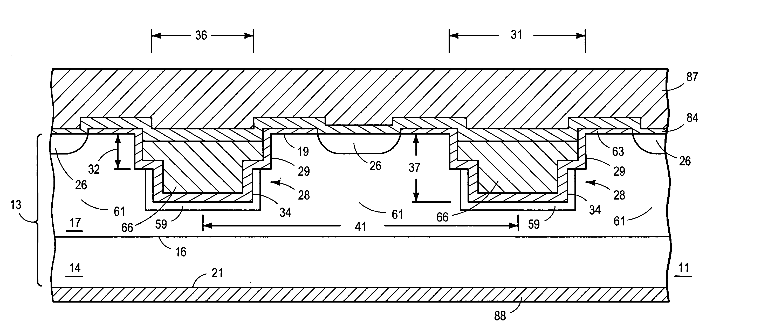
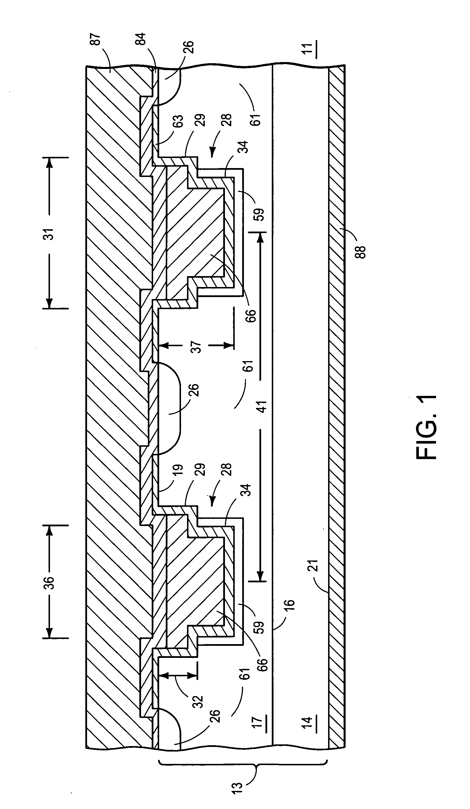
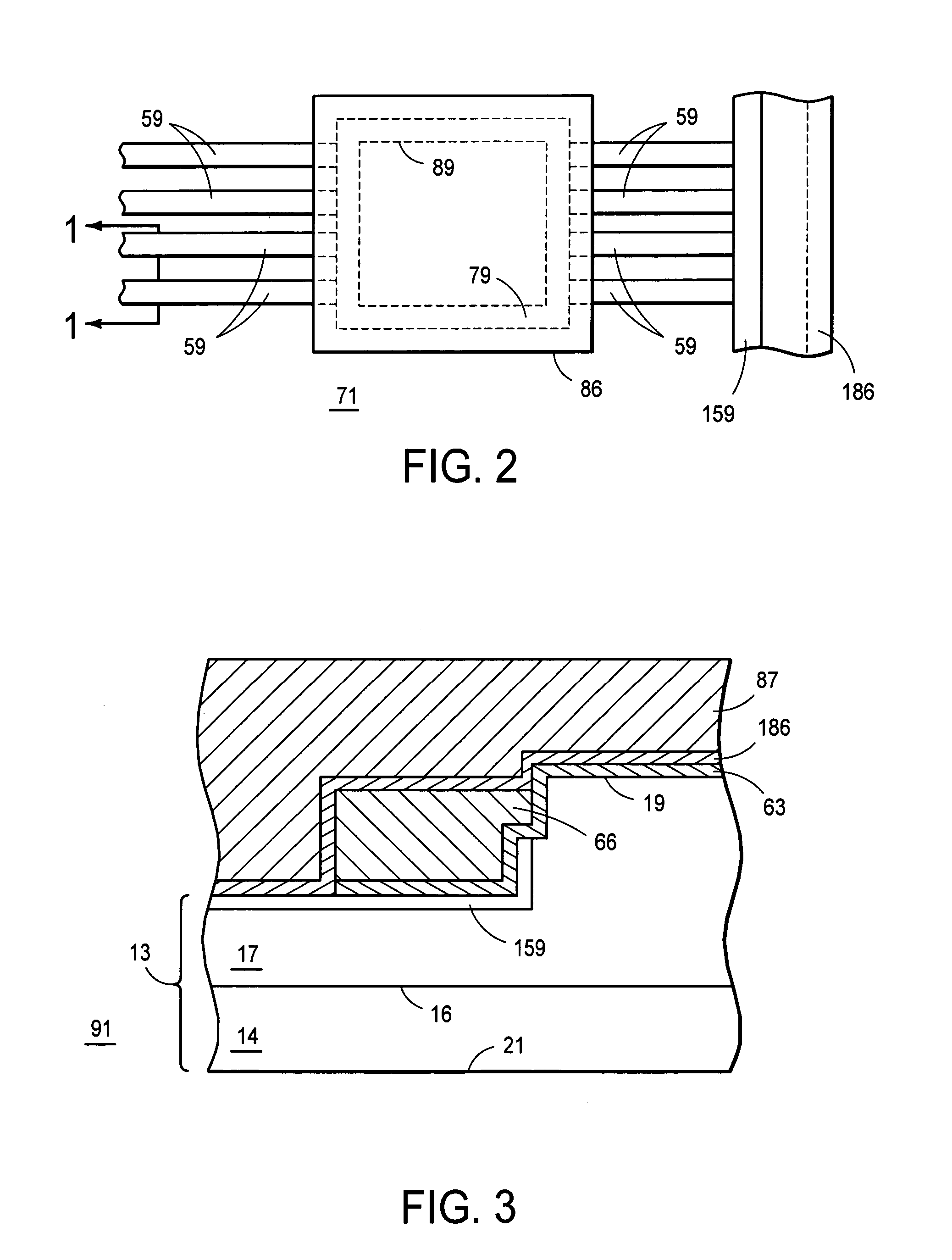
[0018] In general, the present invention pertains to a dc / dc power conversion circuit or network that includes at least one compound semiconductor depletion mode junction field effect transistor (JFET) structure. In a preferred embodiment, the circuit includes at least one GaAs depletion mode FET as a switching device. The switching device reduces gate charging effects, gate resistance effects, reverse recovery times, and on resistance thereby improving power conversion performance.

[0019] Unlike silicon, GaAs is a direct bandgap compound semiconductor material with an inherent property of high electron mobility (8500 cm2 / V-sec), which is greater than 4× that of silicon (1500 cm2 / V-sec). Also, GaAs has a larger bandgap of 1.42 eV compared to 1.1 eV for silicon, which provides, among other things, enhanced performance at elevated temperatures. Additionally, the reverse recovery charge of a GaAs FET device is approximately 100× lower than that of a...


PUM


Abstract

In one embodiment, a dc/dc converter network (71) is described. The converter network (71) includes at least one GaAs depletion mode or normally on FET device (711, 712). The converter network (71) is a two-port system having a positive input terminal (710), a positive output terminal (730), and a negative input terminal (720) connected to a negative output terminal (740). A first GaAs depletion mode FET (711) is connected between the positive input terminal (710) and an internal node (795). A second GaAs depletion mode FET (712) is connected between the internal node (795) and the common negative terminals (720, 740). A control circuit (780) is connected gate leads of the two FETs (711, 712), to alternatively switch the devices from a current conducting mode to a current blocking mode. An inductor (760) is connected between the internal node (795) and the positive output terminal (730). The GaAs depletion mode devices provide a converter network with improved performance.

Description

RELATED APPLICATIONS [0001] This application is related to co-pending U.S. patent application Ser. No. 10 / ______, Attorney Docket No. ONS00501, entitled “VERTICAL COMPOUND SEMICONDUCTOR FIELD EFFECT TRANSISTOR STRUCTURE”, by Peyman Hadizad, assigned to the same assignee, Semiconductor Components Industries, LLC, filed concurrently herewith, and which is incorporated by reference for all purposes. [0002] This application is further related to co-pending U.S. patent application Ser. No. 10 / ______, Attorney Docket No. ONS00505, entitled “METHOD OF MAKING A VERTICAL COMPOUND SEMICONDUCTOR FIELD EFFECT TRANSISTOR DEVICE”, by Peyman Hadizad, assigned to the same assignee, Semiconductor Components Industries, LLC, filed concurrently herewith, and which is incorporated by reference for all purposes.BACKGROUND OF THE INVENTION [0003] This invention relates generally to high frequency power semiconductor applications, and more specifically to dc / dc converters using field effect transistor (FE...

Claims


Application Information

Patent Timeline
IPC IPC(8): H01L27/06H02M3/158
CPCH01L27/0605Y02B70/1466H02M3/1588Y02B70/10
Inventor HADIZAD, PEYMAN
Owner JPMORGAN CHASE BANK NA
Learn More