Lithography apparatus for manufacture of integrated circuits

a technology of integrated circuits and lithography equipment, which is applied in the direction of photomechanical equipment, instruments, originals for photomechanical treatment, etc., can solve the problems of degrading photoresists, material photoresisting, and physical and technical limits of conventional techniques for improving resolution

Active Publication Date: 2005-02-17
TAIWAN SEMICON MFG CO LTD
View PDF30 Cites 709 Cited by
  • Summary
  • Abstract
  • Description
  • Claims
  • Application Information

AI Technical Summary

Benefits of technology

[0022] The preferred embodiment relates to the field of lithographic systems, and more specifically, to immersion lithographic systems that employ an immersion fluid betwee

Problems solved by technology

However, these conventional techniques of improving the resolution are approaching physical and technical limits.
However, conventional immersion f

Method used


Image

  • Lithography apparatus for manufacture of integrated circuits
  • Lithography apparatus for manufacture of integrated circuits
  • Lithography apparatus for manufacture of integrated circuits

Examples


Embodiment Construction

[0034] The making and using of the presently preferred embodiments are discussed in detail below. It should be appreciated, however, that the present invention provides many applicable inventive concepts that can be embodied in a wide variety of specific contexts. The specific embodiments discussed are merely illustrative of specific ways to make and use the invention, and do not limit the scope of the invention.

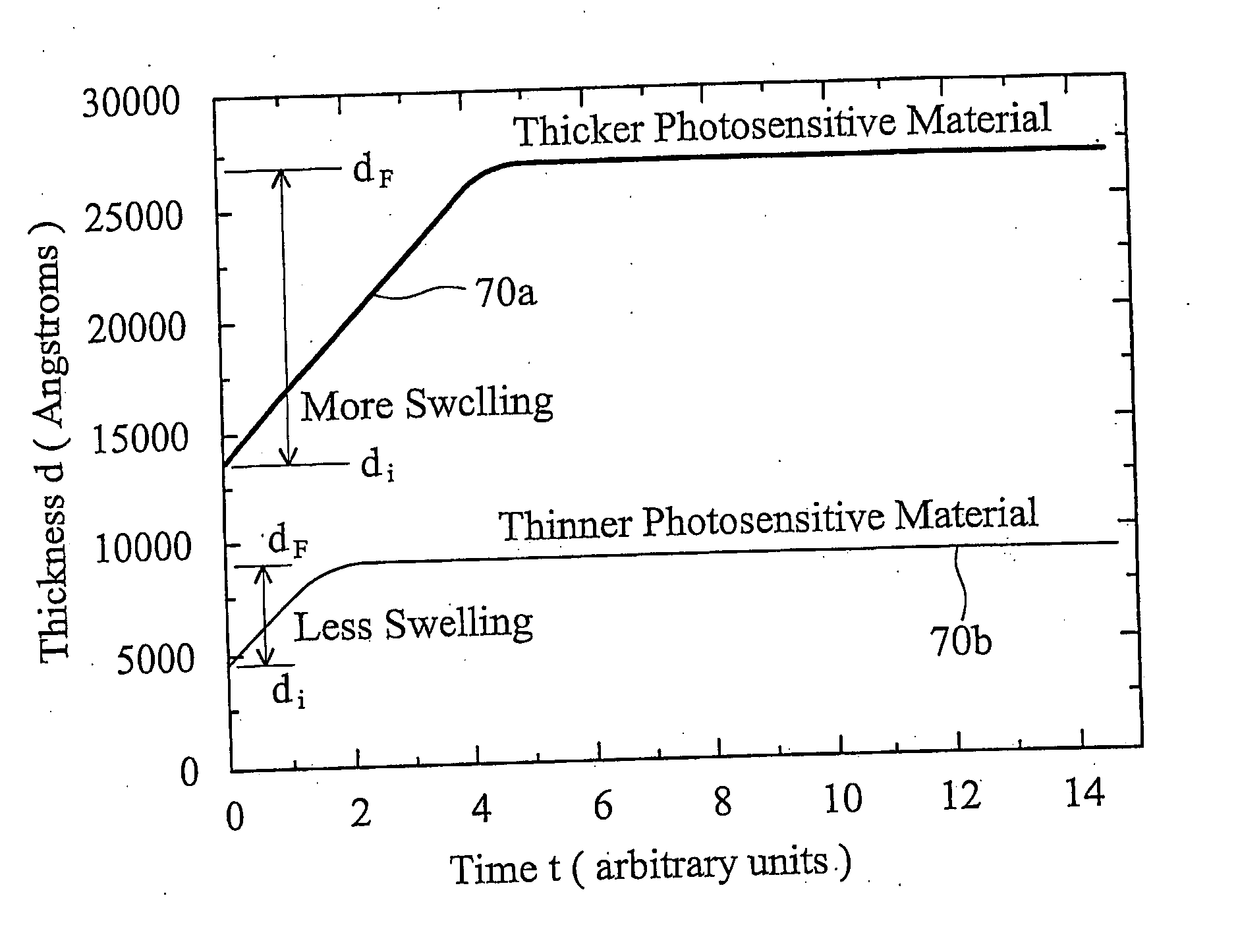
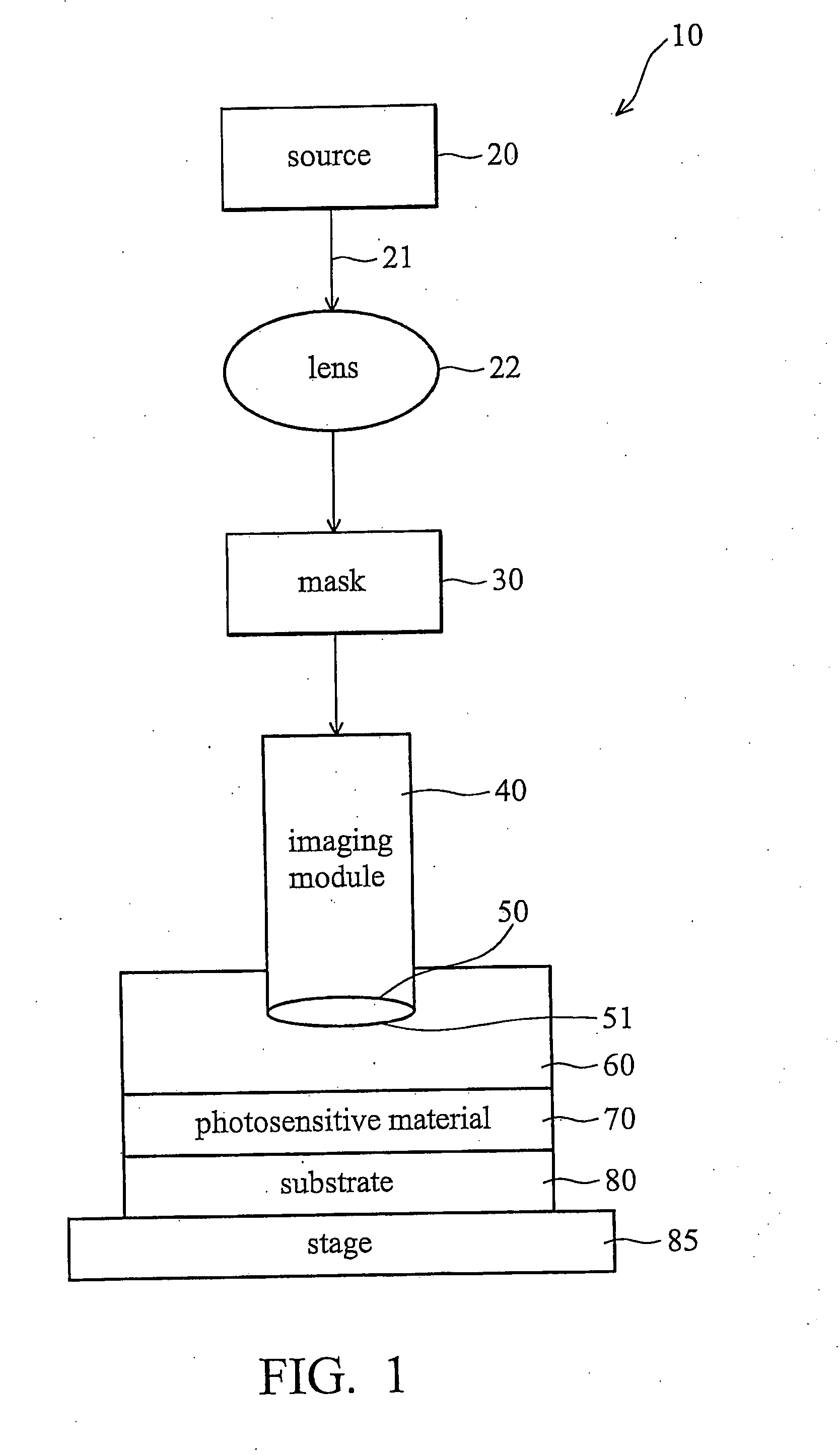
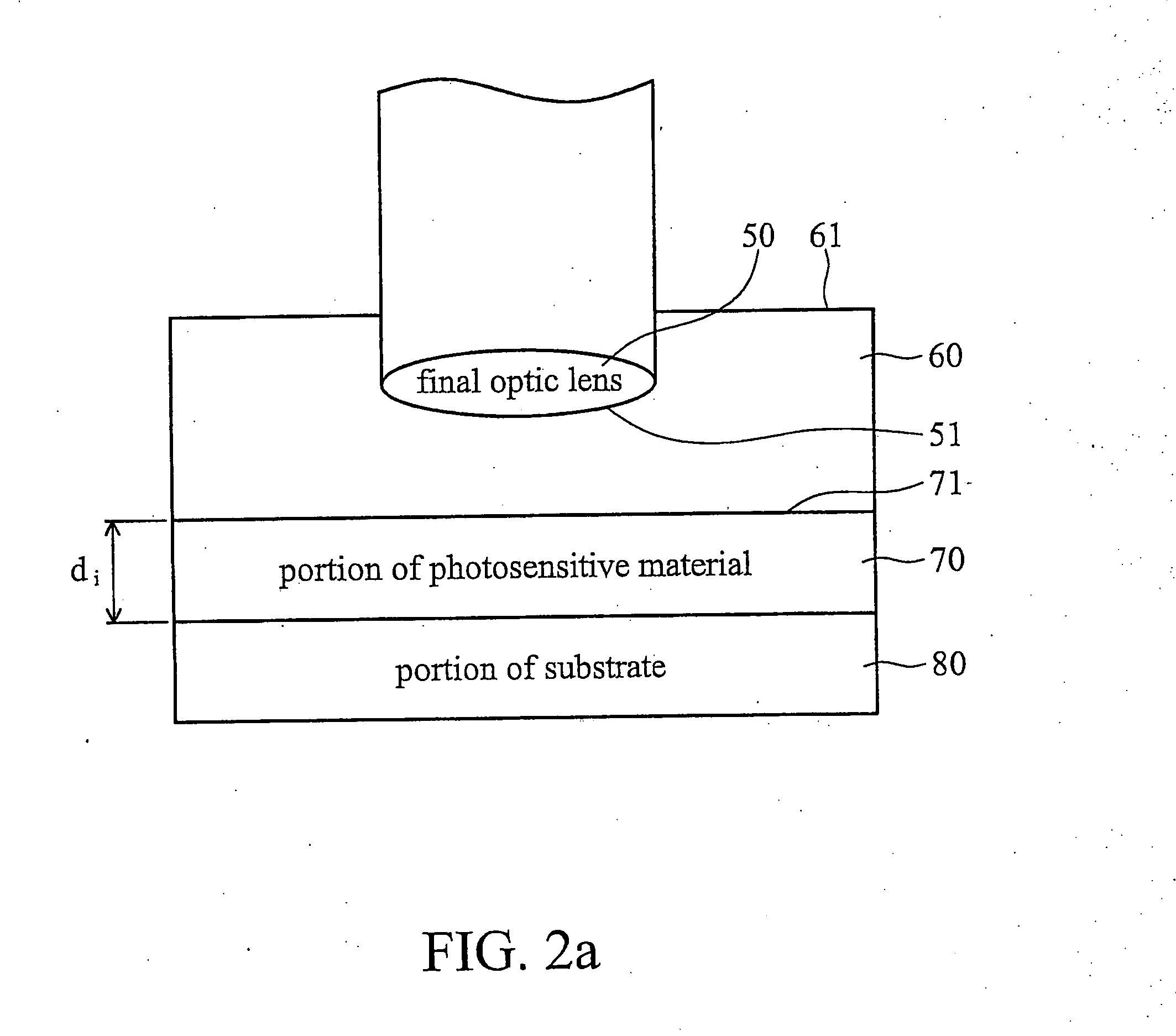
[0035] In an exemplary embodiment of the present invention, shown in FIG. 1, an immersion lithographic system 10 contains a source 20 emitting a beam of optical energy 21 through a lens 22. The energy is then passed through a mask 30 and an imaging module 40, and a final lens 50 having an optical surface 51. In specific embodiments, the lens 50 can be formed from silicon oxide (or another material including silicon and oxygen), fused silica or calcium fluoride, as examples. In one example, the light source 20 can project light having a wavelength of less than or equal to ab...


PUM


Abstract

An immersion lithographic system 10 comprises an optical surface 51, an immersion fluid 60 contacting at least a portion of the optical surface, and a semiconductor structure 80 having a topmost photoresist layer 70 having a thickness of less than about 5000 angstroms, wherein a portion of the photoresist is in contact with the immersion fluid. Further, a method for illuminating a semiconductor structure 80 having a topmost photoresist layer 70 with a thickness of less than about 5000 angstroms, comprising introducing an immersion fluid 60 into a space between an optical surface 51 and the photoresist layer, and directing light preferably with a wavelength of less than about 450 nm through the immersion fluid and onto the photoresist.

Description

CROSS-REFERENCE TO RELATED APPLICATIONS [0001] This application claims priority based on U.S. Provisional Patent Application Ser. No. 60 / 494,154, filed Aug. 11, 2003, entitled “Lithography Apparatus for Manufacture of Integrated Circuits”. The provisional application is incorporated herein by reference in its entirety. [0002] This application is related to U.S. Provisional Application Ser. No. 60 / 498,195, filed Aug. 25, 2003, entitled “Immersion Fluid for Immersion Lithography, and Method of Performing Immersion Lithography”. The application is incorporated herein by reference in its entirety.TECHNICAL FIELD [0003] The present invention relates generally to the fabrication of semiconductor devices, and more specifically, to immersion lithographic systems that employ an immersion fluid between a final optic and a substrate. BACKGROUND [0004] In photolithographic systems, there is a need to achieve a high resolution in order to resolve high-resolution patterns, such as images, lines, ...

Claims


Application Information

Patent Timeline
IPC IPC(8): G03F7/20
CPCG03F7/70341
Inventor YEO, YEE-CHIAHU, CHENMING
Owner TAIWAN SEMICON MFG CO LTD
Why Eureka
Try Eureka