

Optical waveguide having specular surface formed by laser beam machining
a technology of laser beam machining and optical waveguide, which is applied in the direction of optical waveguide light guide, optical waveguide, instruments, etc., can solve the problems of inability to form the optical waveguide to be smaller than a predetermined size or length, and achieve the effect of reducing the size of the optical waveguide, reducing the degree of freedom in designing the optical circuit, and large divergence angl
- Summary
- Abstract
- Description
- Claims
- Application Information
AI Technical Summary
Benefits of technology
Problems solved by technology
Method used
Image

Examples
first embodiment
[0047] (First Embodiment)
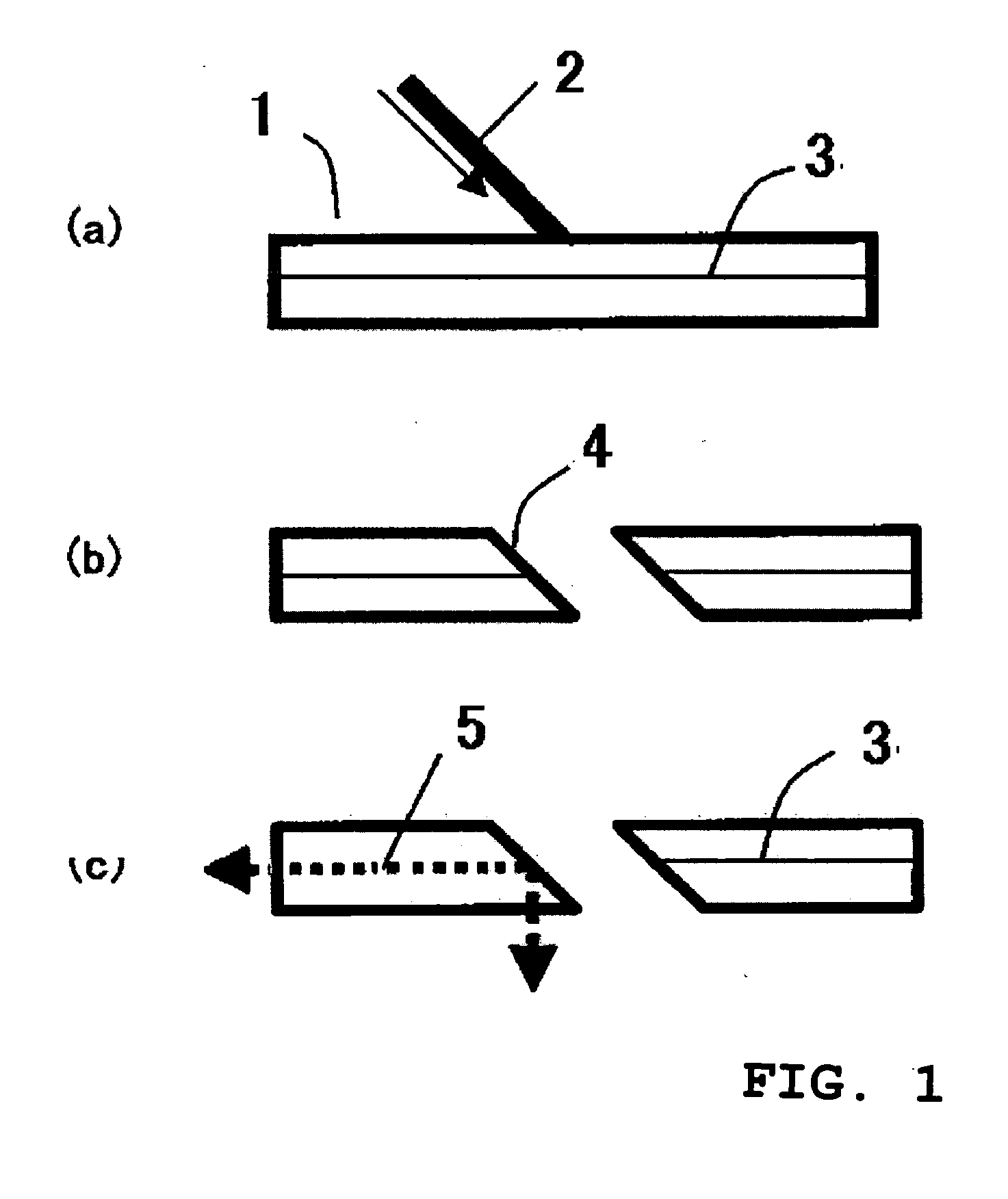
[0048] Polyimide including 2,2-bis(3,4-dicarboxy phenyl) hexafluoropropane 2 anhydride (6FDA) and 2,2-bis(trifluoro methyl)-4,4′-diaminobiphenyl (TFDB) is formed as upper and lower cladding layers on a 5-inch silicon wafer, and polyimide including 6FDA and 4,4′-oxydianiline (ODA) is formed as a core layer disposed between the upper and lower cladding layers. The core on the lower cladding layer is patterned using well-known methods of photolithography and dry etching, and then the upper cladding layer is formed, thereby forming a film-shaped optical waveguide. Here, a plurality of core layers parallel to each other in the longitudinal direction is formed, thereby providing a multi array optical waveguide. Thereafter, the silicon wafer in which the optical waveguide is formed is immersed in an aqueous solution including 5 wt % of hydrofluoric acid and thus the optical waveguide is separated from the silicon wafer, thereby manufacturing a film-shaped optical w...
second embodiment
[0051] (Second Embodiment)
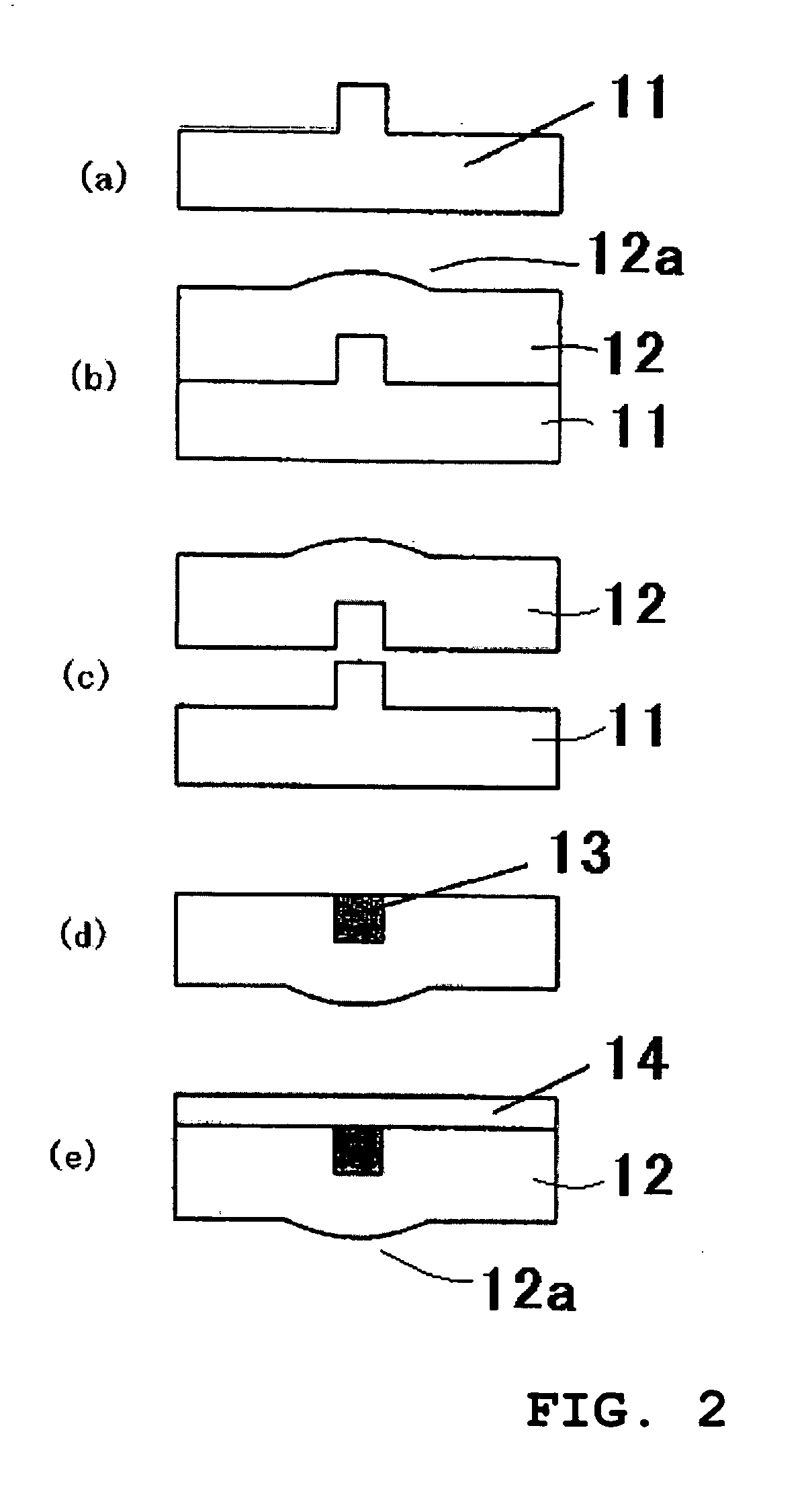
[0052] By dry-etching a 5-inch silicon wafer, a ridge-shaped core pattern having a width of 50 μm and a height of 40 μm is formed. This serves as a mold. A solution of poly(amic acid) including 2,2-bis(3,4-dicarboxy phenyl) hexafluoropropane 2 anhydride (6FDA) and 2,2-bis(trifluoro methyl)-4,4′-diaminobiphenyl (TFDB) is spin-coated thereon and is then made to be polyimide through heat treatment. At this time, the concentration of the solution of poly(amic acid) is set to 25%. A portion protruded along a core pattern is formed on the top surface of the cladding layer on the core pattern. Next, by immersing the cladding layer of polyimide in distilled water, the cladding layer is separated from the silicon wafer. Next, the formed groove is filled with co-polymerized polyimide including 6FDA, 4,4′-oxydianiline (ODA), and 6FDA / TFDB through spin coating and heat treatment. Further, a cladding layer made of 6FDA / TFDB is formed thereon. In this way, the film-shape...
third embodiment
[0055] (Third Embodiment)
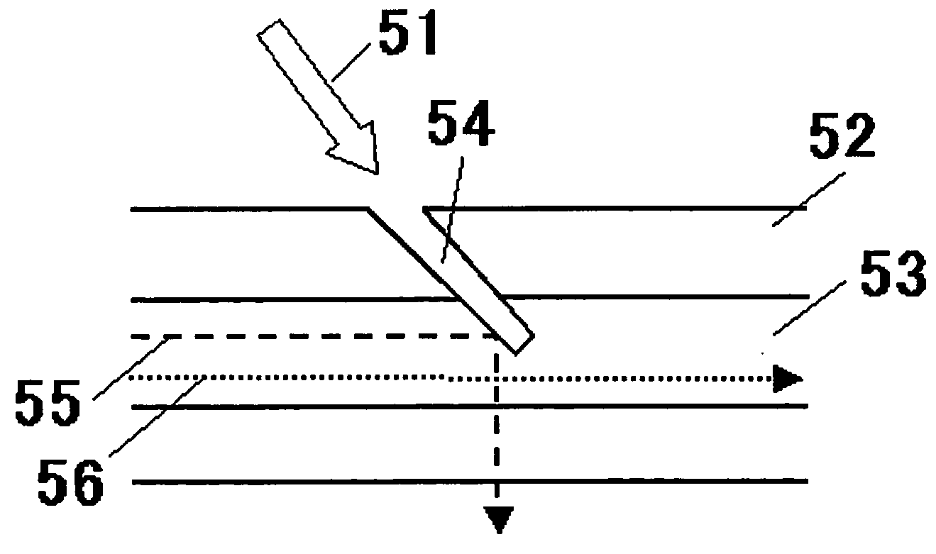
[0056] By forming the upper and lower cladding layers using polyimide including 2,2-bis(3,4-dicarboxy phenyl) hexafluoropropane 2 anhydride (6FDA) and 2,2-bis(trifluoro methyl)-4,4′-diaminobiphenyl (TFDB), forming the core layer using polyimide including 6FDA and 4,4′-oxydianiline (ODA), and performing the well-known methods of photolithography and dry etching thereto, a multimode optical waveguide film is formed on a 5-inch silicon wafer. At this time, the optical waveguide is patterned in a T shape. Thereafter, by immersing the silicon wafer, on which the optical waveguide is formed, in an aqueous solution of 5 wt % of hydrofluoric acid, the optical waveguide is separated from the silicon wafer, thereby forming a film-shaped optical waveguide. The thickness of the film-shaped optical waveguide is set to 80 μm.
[0057] Next, a rectangular through-hole is formed at the intersection of the T shape using a reduction optical system-mask projecting KrF excimer la...
PUM
 Abstract
Description
Claims
Application Information