High-resolution variable attenuation device

a variable attenuator and high-resolution technology, applied in the field of attenuators, can solve the problems of increasing the parts count of the attenuator unit, requiring time and cost calibration, and providing non-linear performance of voltage-variable and pin-diode attenuators, and achieve the effect of uniform attenuation steps of the input signal

Inactive Publication Date: 2005-05-05
LTX CORP
View PDF5 Cites 19 Cited by
  • Summary
  • Abstract
  • Description
  • Claims
  • Application Information

AI Technical Summary

Benefits of technology

[0007] According to an aspect of this invention, a variable attenuation device includes a resistive array having two or more input nodes, two or more output nodes, and two or more resistive devices for coupling the input nodes and the output nodes. A first switch has an input terminal and two or more selectable output terminals, such that the input terminal is configured to receive an input signal and the two or more selectable output terminals are coupled to the two or more input nodes of the resistive array. A second switch has two or more selectable input terminals and an output terminal, such that the output terminal is configured to provide an attenuated output signal and the two or more selectable input terminals are coupled to the two or more output nodes of the resistive array. The output terminal selected on the first switch and the input terminal selected on the second switch varies the resistance seen by the input signal, and the values of the two or more resistive devices are configured to allow for substantially uniform attenuation steps of the input signal.

Problems solved by technology

Unfortunately, even with digital control, voltage-variable and PIN-diode attenuators provide non-linear performance, require time and cost to calibrate, and increase the parts count per attenuator unit.
While digital attenuators allow for direct digital control, these attenuators are typically too coarse, in that the highest-resolution achievable (i.e., the smallest amount of attenuation selectable) is between 0.25 and 0.50 decibels.

Method used


Image

  • High-resolution variable attenuation device
  • High-resolution variable attenuation device
  • High-resolution variable attenuation device

Examples


Embodiment Construction

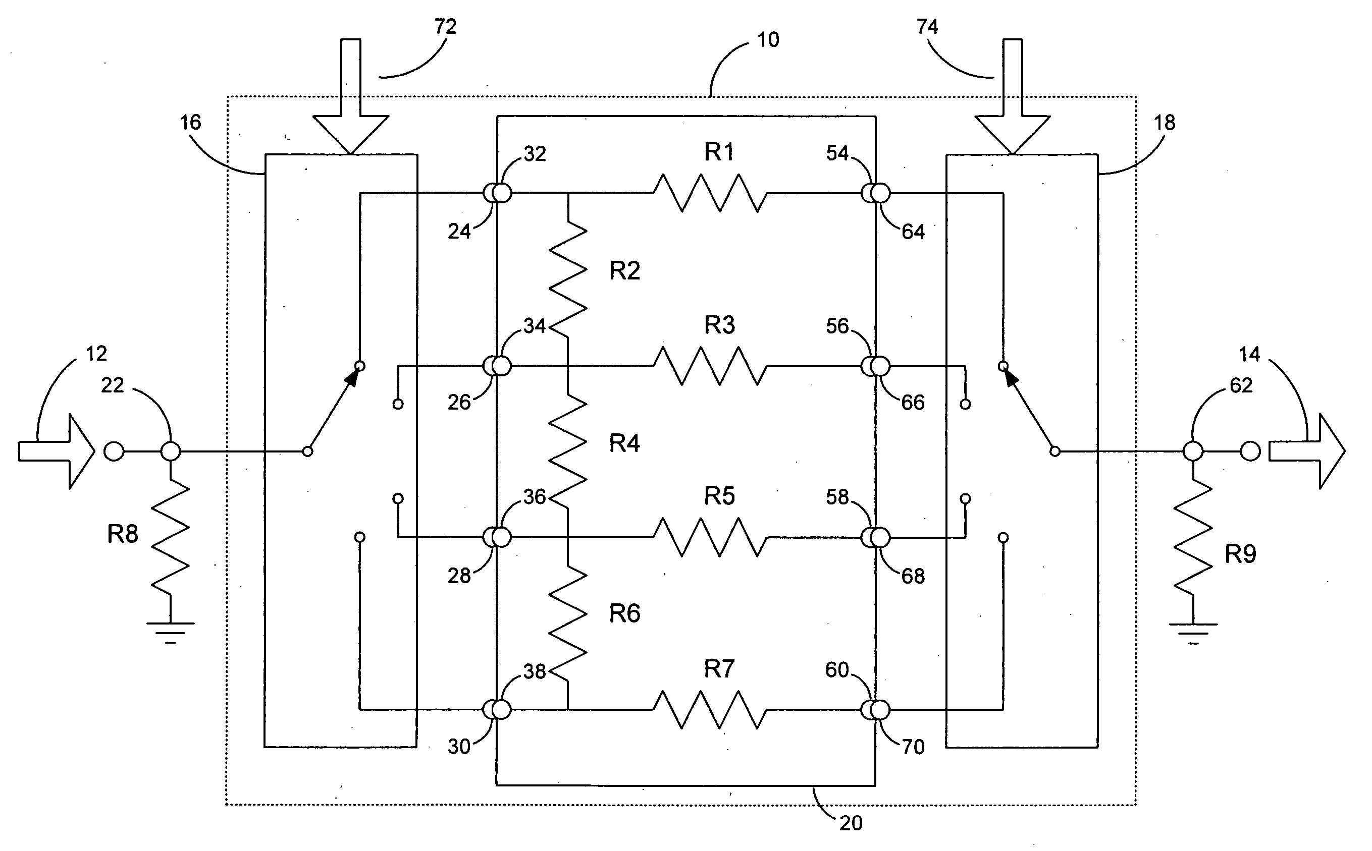
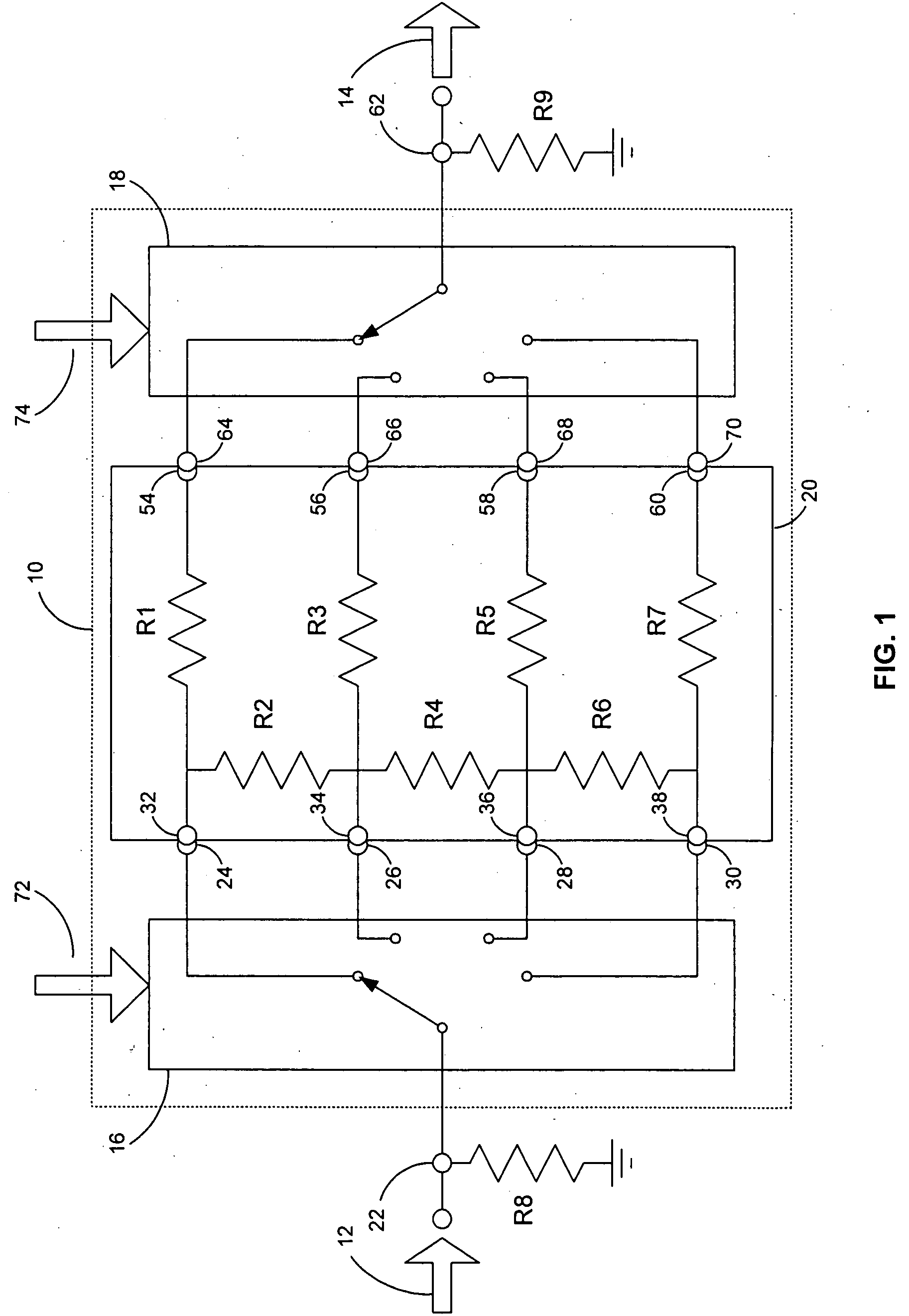
[0029] Referring to FIG. 1, there is shown a variable attenuation device 10 for receiving a input signal 12, such as an RF (i.e., radio frequency) or microwave signal and providing an attenuated output signal 14. (030) Variable attenuation device 10 includes a first switch 16, a second switch 18, and a resistive array 20. As will be discussed below, by controlling the position of switches 16 and 18, the level of attenuation experienced by input signal 12 is controllable.

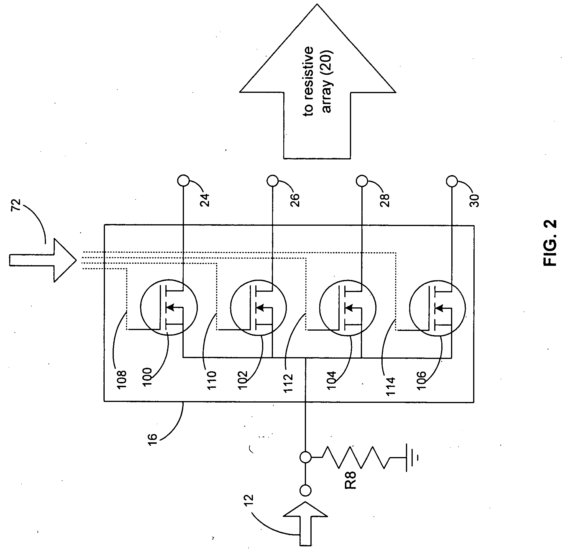
[0030] First switch 16 includes an input terminal 22 and four selectable output terminals 24, 26, 28 and 30. Output terminals 24, 26, 28 and 30 are coupled to the input nodes 32, 34, 36 and 38 of resistive array 20.

[0031] Resistive array 20 includes multiple resistors R1-R7 that provide resistive paths between input nodes 32, 34, 36 and 38 and output nodes 54, 56, 58 and 60 of resistive array 20. These resistors may be connected between an input and an output node (e.g., resistor R1), between input nodes (e.g., res...


PUM


Abstract

A variable attenuation device includes a resistive array having two or more input nodes, two or more output nodes, and two or more resistive devices for coupling the input nodes and the output nodes. A first switch has an input terminal and two or more selectable output terminals, such that the input terminal is configured to receive an input signal and the two or more selectable output terminals are coupled to the two or more input nodes of the resistive array. A second switch has two or more selectable input terminals and an output terminal, such that the output terminal is configured to provide an attenuated output signal and the two or more selectable input terminals are coupled to the two or more output nodes of the resistive array. The output terminal selected on the first switch and the input terminal selected on the second switch varies the resistance seen by the input signal, and the values of the two or more resistive devices are configured to allow for substantially-uniform attenuation steps of the input signal.

Description

FIELD OF THE INVENTION [0001] This invention relates to attenuators and, more particularly, to digital planar RF attenuators. BACKGROUND [0002] When verifying the proper operation of circuitry components, test equipment is often used to generate test signals that are provided to the components being tested. In order to ensure accurate verification, the characteristics of these test signals have to be controlled. Examples of these signal characteristics are signal type (e.g., DC, AC, sine wave, square wave, etc.), signal frequency, frequency sweep rate, signal amplitude, and amplitude sweep rate. [0003] Variable attenuators are often used to control signal amplitude. Examples of these variable attenuators include voltage-variable analog attenuators, PIN-diode attenuators, and digital attenuators (e.g., switched-bit digital attenuators). [0004] Voltage-variable analog attenuators typically include one or more field effect transistors that are controlled (via their gate voltage) to act...

Claims


Application Information

Patent Timeline
Patent Type & Authority Applications(United States)
IPC IPC(8): H03H7/25H03H11/24H03L5/00
CPCH03H11/245H03H7/25
Inventor KAISER, JOSEPH A. JR.
Owner LTX CORP
Why Eureka
Try Eureka