Memory system having flash memory where a one-time programmable block is included

a memory system and one-time programmable block technology, applied in static storage, digital storage, instruments, etc., can solve the problems of data stored in the otp block being damaged by non-permitted users, the complexity of information process systems has increased, and the flash memory device with the otp block and the memory system including the same undergo some problems, so as to achieve the effect of cutting off the access

Inactive Publication Date: 2005-05-19
SAMSUNG ELECTRONICS CO LTD
View PDF4 Cites 31 Cited by
  • Summary
  • Abstract
  • Description
  • Claims
  • Application Information

AI Technical Summary

Benefits of technology

[0024] According to another feature of the present invention, the memory system comprises a flash memory device including an OTP block where the protection data information is stored in a predetermined region and an interface device including a register for storing OTP lock status information for indicating whether the OTP block is programmed. The flash memory device comprises a memory block, a memory block selection circuit for selecting the memory block, an OTP block selection circuit for selecting the OTP block, and a control circuit for setting the memory block selection circuit to an inactive state and the OTP block selection circuit to an active state, respectively, so as to cut off an access to the memory block in the OTP mode.
[0025] In this embodiment, when a program / erase command is externally applied in the OTP mode, the interface device has OTP lock status information indicating whether the OTP block is programmed. When the OTP lock status information indicates that the OTP block is programmed, the interface device cuts off an external access to the OTP block. The access to the OTP block includes a program / erase operation of the OTP block. When the OTP lock status information indicates that the OTP block is not programmed, the interface device outputs a command for notifying the memory device of an entry to the OTP mode. The control circuit sets the memory block selection circuit to an inactive state and the OTP block selection circuit to an active state in response to the command, respectively, for notifying an entry to the OTP mode.

Problems solved by technology

Recently, as the complexity of information process systems has increased, the users want to store device ID data, such as a serial number of the product company, a manufacture date, security-required data, and the like, in the flash memory device together with the public data.
However, the flash memory device with the OTP block and the memory system including the same undergo some problems.
1) In the case that a program operation for the OTP block is allowed, data stored in the OTP block may be damaged by a non-permitted user if the program command is known.
Therefore, the important security data stored in the OTP block may be damaged.
2) To identify whether the OTP block is programmed has a difficulty of always accessing (or reading) the OTP block.
However, the technique disclosed in the above patent requires additional fuses and a process for cutting the fuses.

Method used


Image

  • Memory system having flash memory where a one-time programmable block is included
  • Memory system having flash memory where a one-time programmable block is included
  • Memory system having flash memory where a one-time programmable block is included

Examples


first embodiment

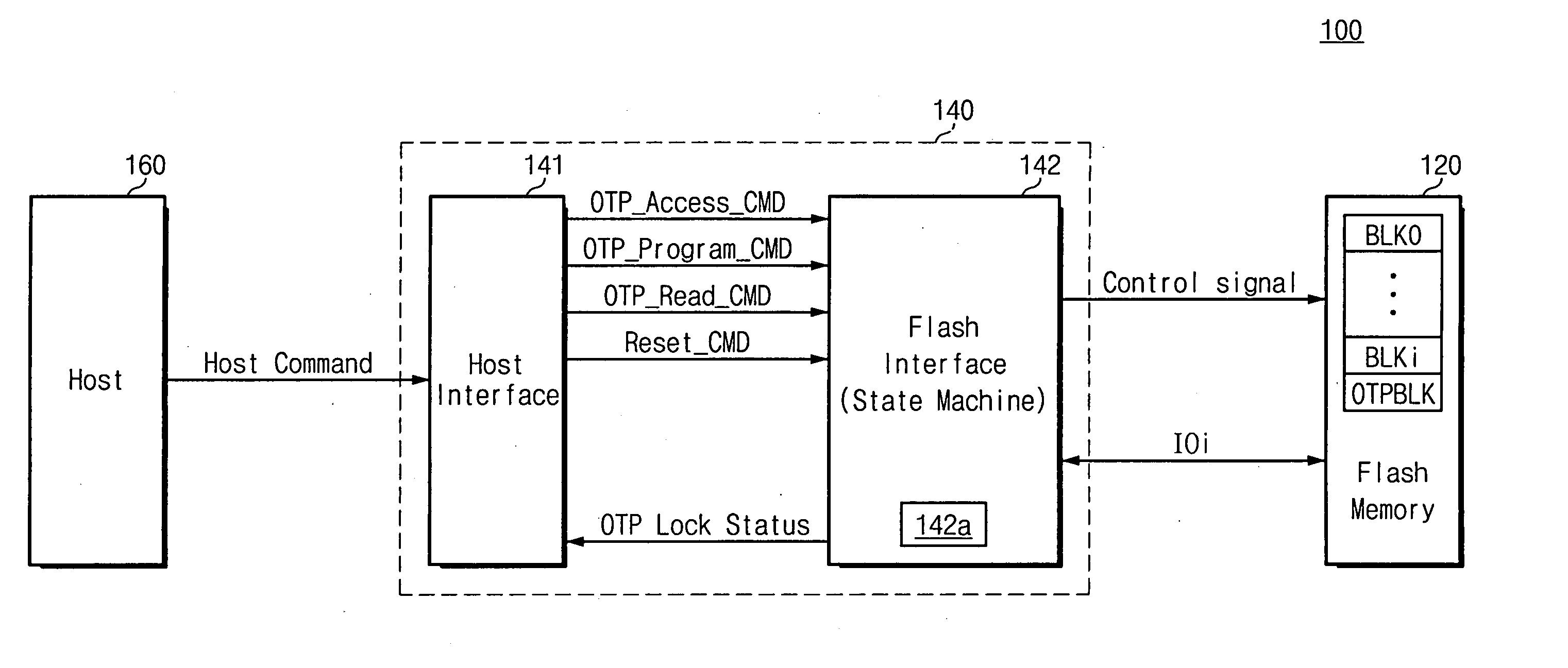
[0033]FIG. 1 is a schematic diagram block of a memory system according to the present invention. Referring to FIG. 1, the memory system 100 of the present invention includes a flash memory device 120, an interface device 140, and a host 160. The flash memory device 120 includes a storage region for storing data, which is comprised of a plurality of memory blocks BLK0-BLKi and at least one OTP block OTPBLK. In the present invention, erase / program / read operations for the memory blocks BLK0-BLKi and a read operation for the OTP block OTPBLK are not limited. Contrary to this, the erase / program operations for the OTP block OTPBLK are limited, which will be fully explained herein. Each of the memory blocks BLK0-BLKi and the OTP block OTPBLK comprises electrically erasable and programmable ROM cells (EEPROMs), each of which has a floating gate transistor.

[0034] The interface device 140 serves as an interface between the flash memory device 120 and the host 160. The interface device 140 inc...

second embodiment

[0055]FIG. 5 is a schematic block diagram of a memory system according to the present invention. In FIG. 5, constituent elements that are identical with those in FIG. 1 are marked by the same numerals, and description thereof is thus omitted.

[0056] In the case of a memory system according to the first embodiment of the present invention, as described above, protection data indicating whether an OTP block is programmed is stored in the OTP block together with security data. Furthermore, in the case of the memory system according to the second embodiment of the present invention, test information (e.g., an operating frequency of a flash memory device) obtained at a package level is stored in the OTP block OTPBLK. The test information is stored in any address region of the OTP block (e.g., a main area or a spare region of the OTP block) at a package test level before the security and protection data is stored therein.

[0057] Referring to FIG. 5, an interface device 140 includes a host ...


PUM


Abstract

A memory system includes a flash memory device and an interface device. The flash memory device includes a one-time programmable block where protection data information is stored in a predetermined region, and the interface device includes a register for storing one-time programmable lock status information to indicate whether the one-time programmable block is programmed. When a program/erase command is applied externally in a one-time programmable mode, the interface device having the one-time programmable lock status information indicates whether the one-time programmable block is programmed. If the one-time programmable lock status information indicates that the one-time programmable block is programmed, the interface device cuts off an external access to the one-time programmable block.

Description

[0001] This application claims priority from Korean Patent Application No. 2003-80301, filed on Nov. 13, 2003 and Korean Priority Application No. 2004-31117, filed on May 3, 2004, the contents of which are herein incorporated by reference in its entirety. BACKGROUND OF THE INVENTION [0002] 1. Field of this Invention [0003] This disclosure relates to a semiconductor memory device, and more particularly, to a flash memory device including a one-time programmable block (hereinafter, referred to as ‘OTP block’). [0004] 2. Description of Prior Art [0005] Electrically erasable and programmable flash memory devices have been used in various applications. The flash memory device stores data requiring no security (hereinafter, referred to as public data) and includes a memory cell array of EEPROM cells. Recently, as the complexity of information process systems has increased, the users want to store device ID data, such as a serial number of the product company, a manufacture date, security-...

Claims


Application Information

Patent Timeline
Patent Type & Authority Applications(United States)
IPC IPC(8): G11C16/02G11C11/34G11C16/04G11C16/22
CPCG11C2216/26G11C16/22
Inventor LEE, CHUL-HOCHO, HYUN-DUKKIM, CHANG-RAE
Owner SAMSUNG ELECTRONICS CO LTD
Why Eureka
Try Eureka