

Semiconductor device fabrication method and apparatus
a technology of semiconductor devices and fabrication methods, applied in the direction of manufacturing tools, grinding machines, lapping machines, etc., can solve the problems of complex cleaning process, increased size of attached apparatuses, and no inexpensive, effective cleaning member which can be easily attached
- Summary
- Abstract
- Description
- Claims
- Application Information
AI Technical Summary
Problems solved by technology
Method used
Image

Examples
first embodiment
(1) First Embodiment
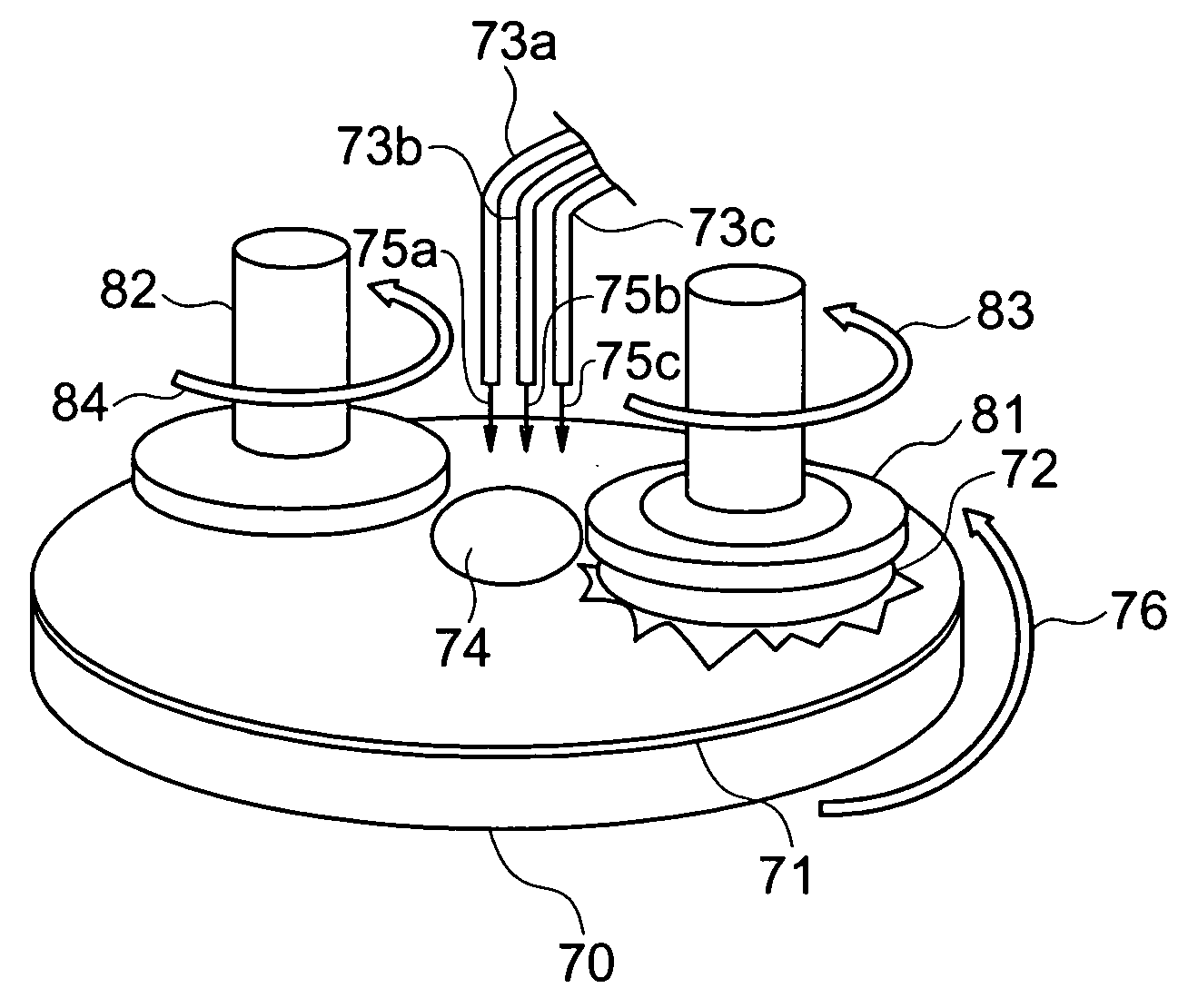
[0031] A semiconductor device fabrication apparatus and method according to the first embodiment of the present invention will be explained below.
[0032]FIG. 1 shows the arrangement of a fabrication apparatus capable of polishing or cleaning according to the first embodiment.
[0033] A pad 71 is placed on a turntable 70 which rotates in the direction of an arrow 76. A filter 74 is adhered on the surface of a central portion of the pad 71. It is also possible to form a hole in the central portion of the pad 71, and embed the filter 74 in this hole.
[0034] The pad 71 can be formed of a porous material having open cells. More specifically, the pad 71 can be formed of, e.g., a polymer-based material such as polyurethane or polypropylene.
[0035] The filter 74 is a sponge-like filter coated with a paste obtained by mixing a solvent, binder, or the like in grains (to be referred to as tourmaline grains hereinafter) of tourmaline as an example of a polar crystal.
[0036] A...
second embodiment
(2) Second Embodiment
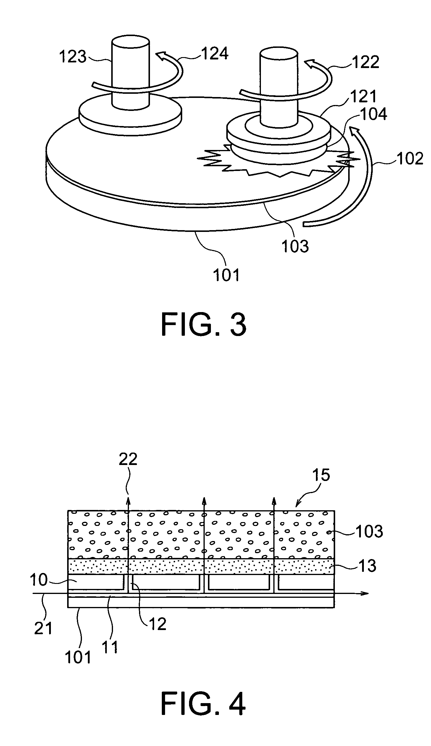
[0064] The second embodiment of the present invention will be described below with reference to the accompanying drawings.
[0065]FIG. 3 shows an outline of the overall arrangement of a polishing apparatus.
[0066] Polishing cloth (a pad) 103 is placed on a turntable 101 which rotates in the direction of an arrow 102, and a semiconductor wafer, for example, is set as an object 104 to be polished.
[0067] As will be described later, a slurry is supplied inside the turntable 101 and discharged to its surface, and the discharged slurry is supplied to the surface to be polished of the object 104 through the polishing cloth 103.
[0068] A top ring head 121 as a holding member or as a pressing mechanism which presses the polishing cloth 103 holds the object 104, and rotates the object 104 while pressing it against the polishing cloth 103. Also, a dressing head 123 for dressing the polishing cloth 103 opposes the top ring head 121 on the other side of the center of the tur...
third embodiment
(3) Third Embodiment
[0082] A cleaning apparatus and method will be described below as a semiconductor fabrication apparatus and method, respectively, according to the third embodiment of the present invention.
[0083] The third embodiment uses a pressure as in the second embodiment, but uses no polishing table.
[0084] As shown in FIG. 5, a semiconductor wafer 41 is supported by a plurality of rollers 55. When the rollers 55 rotate in the direction of an arrow 56, the semiconductor wafer 41 rotates in the direction of an arrow 51. Rolls 42 and 43 are arranged on the two surfaces of the semiconductor wafer 41, and rotate in opposite directions indicated by arrows 52 and 53, respectively.
[0085] As will be described later, each of the rolls 42 and 43 contains a filter, and also functions as a pressing mechanism which applies a pressure to this filter. FIG. 6 shows the sectional structure of each of the rolls 42 and 43.
[0086] A sponge-like, ring-shaped elastic member 61 is formed on the...
PUM
| Property | Measurement | Unit |
|---|---|---|
| grain size | aaaaa | aaaaa |
| grain size | aaaaa | aaaaa |
| grain size | aaaaa | aaaaa |
Abstract
Description
Claims
Application Information