Check patentability & draft patents in minutes with Patsnap Eureka AI!

Circuit interconnect for optoelectronic device

a circuit interconnect and optoelectronic technology, applied in the association of printed circuit non-printed electric components, instruments, optical elements, etc., can solve problems such as deteriorating data signal integrity at high frequencies

Inactive Publication Date: 2005-06-02
II VI DELAWARE INC
View PDF14 Cites 5 Cited by
  • Summary
  • Abstract
  • Description
  • Claims
  • Application Information

AI Technical Summary

Problems solved by technology

Conventional signal and ground connections to TO packages, which including distinct signal and ground connections, result in uncontrolled impedances that degrade data signal integrity at high frequencies (e.g., at or above 3 GHz).

Method used


Image

  • Circuit interconnect for optoelectronic device
  • Circuit interconnect for optoelectronic device
  • Circuit interconnect for optoelectronic device

Examples


Embodiment Construction

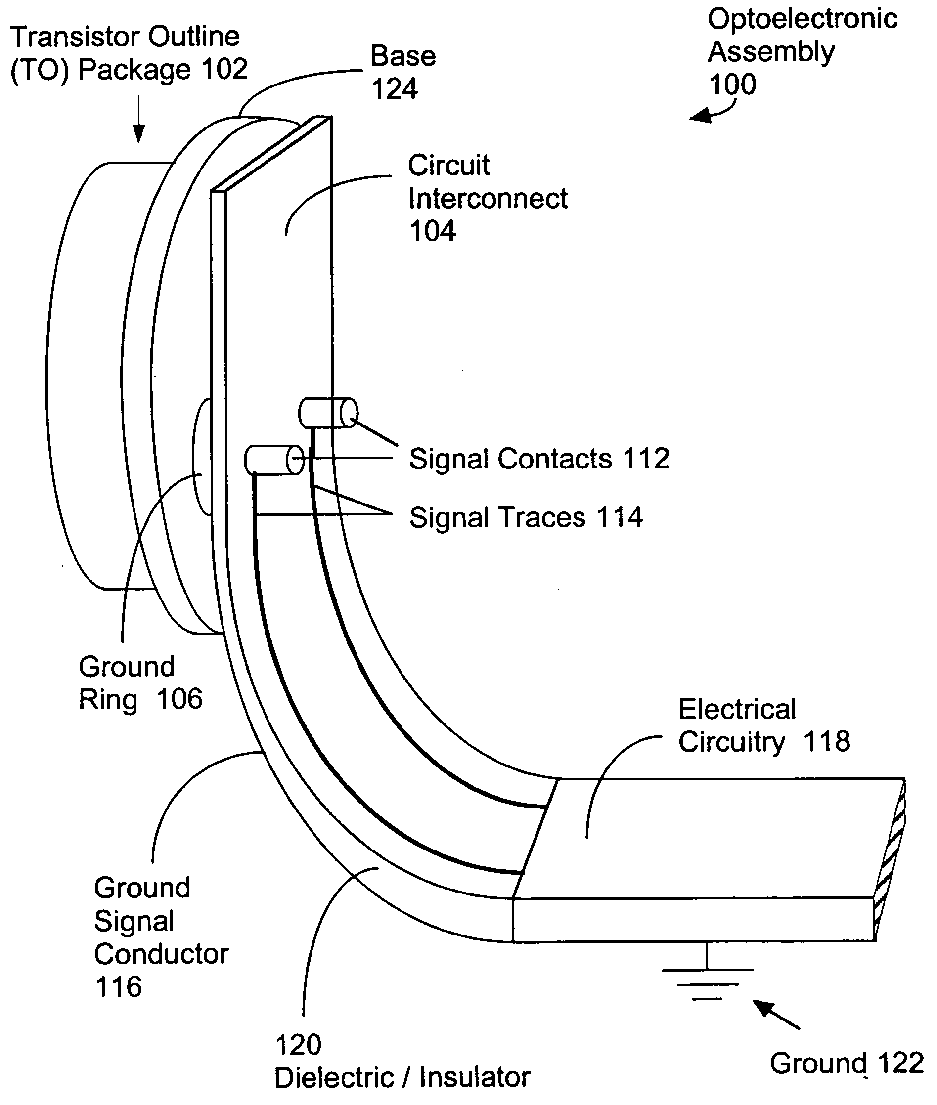
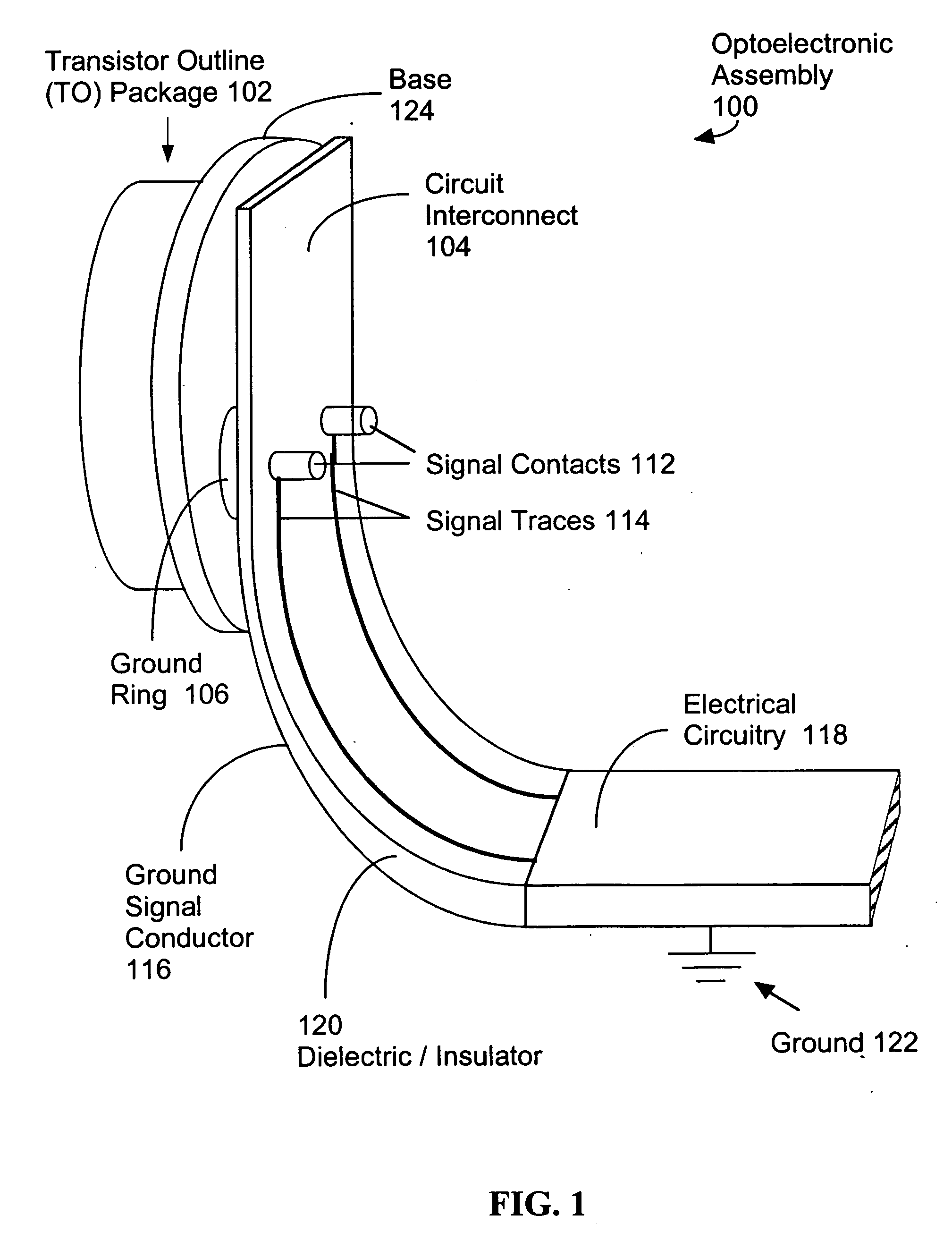
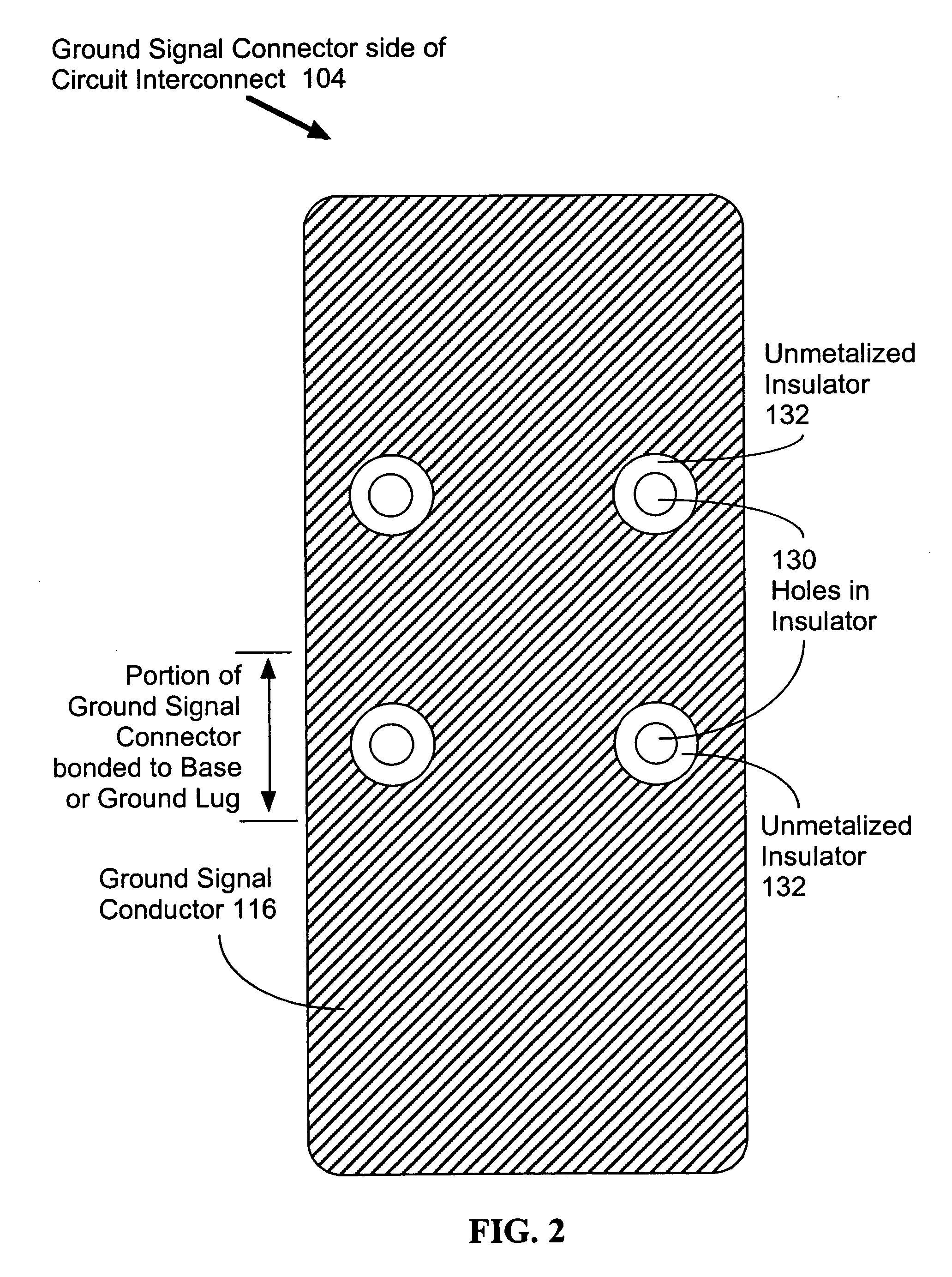
[0004] In general, exemplary embodiments of the invention are concerned with systems and devices configured to implement impedance matching schemes in a high speed data transmission environment. In one example, an optoelectronic assembly is provided that includes a TO package having a base through which one or more leads pass. The leads are electrically coupled to an optoelectronic device in the TO package, and are electrically isolated from the base. Some or all of the leads include a ground ring that is electrically isolated from the lead and electrically coupled with the base. A circuit interconnect is also included that is electrically coupled to the optoelectronic device and the TO package. The circuit interconnect includes a dielectric substrate having signal traces that are electrically coupled to the signal leads. A ground signal conductor disposed on the dielectric substrate is electrically coupled with the ground rings.

BRIEF DESCRIPTION OF THE DRAWINGS

[0005] Additional ob...


PUM


Abstract

This disclosure concerns systems and devices configured to implement impedance matching schemes in a high speed data transmission environment. In one example, an optoelectronic assembly is provided that includes a TO package having a base through which one or more leads pass. The leads are electrically coupled to an optoelectronic device in the TO package, and are electrically isolated from the base. Some or all of the leads include a ground ring that is electrically isolated from the lead and electrically coupled with the base. A circuit interconnect is also included that is electrically coupled to the optoelectronic device and the TO package. The circuit interconnect includes a dielectric substrate having signal traces that are electrically coupled to the signal leads. A ground signal conductor disposed on the dielectric substrate is electrically coupled with the ground rings.

Description

[0001] The present invention relates generally to optoelectronic devices, and particularly to a circuit interconnect for controlled impedance at high frequencies. BACKGROUND OF THE INVENTION [0002] An optoelectronic device, such as a laser diode or a photo diode, is generally enclosed in a transistor outline (TO) package, which provides a conductive housing for the optoelectronic device. A laser diode converts an electrical signal into an optical signal for transmission over a fiber optic cable, while a photo diode converts an optical signal into an electrical signal. In order for a laser diode to convert an electrical signal into an optical signal, the electrical signal must be sent through the TO package of the laser diode. Similarly, an electrical signal from a photo diode must be sent through the TO package of the photo diode to external electrical circuitry. For high frequency operation, it is important to control the impedance seen by the electrical signals that flow into and ...

Claims


Application Information

Patent Timeline
Patent Type & Authority Applications(United States)
IPC IPC(8): G02B6/42H05K1/02H05K1/18H05K3/34
CPCG02B6/4201H01L24/45H01L2924/30107H01L2924/01028H01L2924/01013H01L2224/48091H05K2203/1147H01L2224/45144H01L2924/01079H01L2924/14H01L2924/19041H01L2924/3011H05K1/0243H05K1/189H05K3/3447H05K2201/0715H05K2201/10121H05K2201/10166H05K2201/10371H01L2924/00014H01L2924/00H01L2924/12042H01L2224/48137H01L2224/05554H01L2224/49111H01L2224/49175
Inventor ROSENBERG, PAUL K.CASE, DANIEL K.LIPSON, JANHOFMEISTER, RUDOLF J.NGUYEN, THE' LINH
Owner II VI DELAWARE INC
Features
  • R&D
  • Intellectual Property
  • Life Sciences
  • Materials
  • Tech Scout
  • Unparalleled Data Quality
  • Higher Quality Content
  • 60% Fewer Hallucinations
Learn More