Single-crystal-silicon 3D micromirror

a single crystal, 3d technology, applied in the direction of optics, instruments, optical light guides, etc., can solve the problem of more challenges

Inactive Publication Date: 2005-06-23
AGENCY FOR SCI TECH & RES
View PDF6 Cites 65 Cited by
  • Summary
  • Abstract
  • Description
  • Claims
  • Application Information

AI Technical Summary

Benefits of technology

[0007] A principal object of the present invention is to provide an effective and very manufacturable method of fabricating a 3D free space micromirror device.

Problems solved by technology

However, it is more challenging from a packaging and fiber coupling alignment point of view.

Method used


Image

  • Single-crystal-silicon 3D micromirror
  • Single-crystal-silicon 3D micromirror
  • Single-crystal-silicon 3D micromirror

Examples


Embodiment Construction

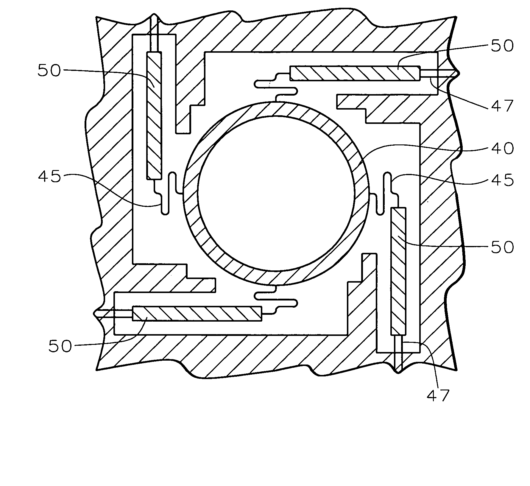
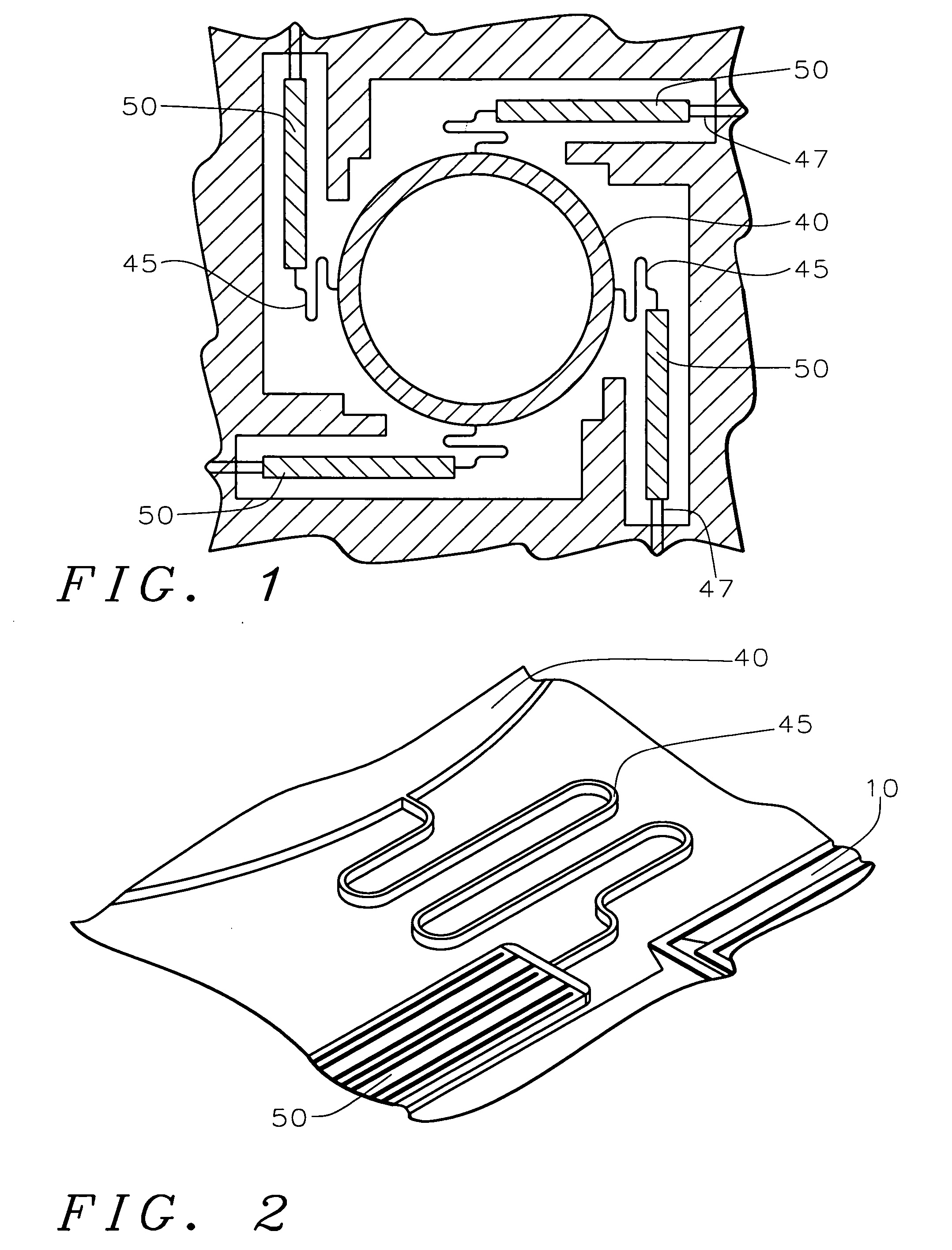
[0020] The present invention discloses a novel design and process for making a 3D free space micromirror device with thick mirror and thin flexible springs and actuators which are monolithically fabricated from a single crystal silicon substrate. Key features of the present invention include the use of 1) a thermal actuator fabricated by a unique process sequence, 2) thin silicon for springs and the actuator and thick silicon for the mirror plate, 3) one monolithic process sequence for fabrication of the actuator, spring, and mirror, and 4) five masking steps, making the process simple and less cumbersome. Silicon is the core material for all components. Silicon dioxide and aluminum are used respectively for electrical isolation and thermal actuation purposes only.

[0021] Top and three-dimensional views of the device can be seen in FIGS. 1 and 2, respectively. The mirror plate 40 is joined with actuators 50 through four flexural springs 45 at four corners 5, symmetrically. Other end...


PUM


Abstract

In a 3D free space micromirror device, a mirror plate is joined with actuators through flexible springs where the other ends of the actuators have fixed support on the substrate. Single crystal silicon and aluminum are used as bi-morph materials with silicon dioxide providing electrical isolation between the two. Thickness variation in the microstructure is achieved by two-step p-n junction formed in a p-type substrate. Thick and thin n-silicon layer formation and DRIE cut mechanisms are employed in such a way that all the thick and thin silicon components of the structure are released simultaneously avoiding overetch which can be detrimental to the thin flexural springs. Working prototypes of the device have been found suitable for any optical switching array architecture where deflections up to 10 degrees are required.

Description

BACKGROUND OF THE INVENTION [0001] (1) Field of the Invention [0002] The invention relates to a method of manufacturing a 3D micromirror, and more particularly, to a method of manufacturing a 3D micromirror using a silicon micro-machining process. [0003] (2) Description of the Prior Art [0004] Micromirror devices based on MEMS technology had a humble debut in the late eighties as display devices. However, a spurt in research activities took place in the mid to late nineties after they were identified as most promising candidates for futuristic all-optical communication networks. There are two basic configurations for micromirror arrays based on MEMS technology, namely 2D in-plane and 3D free space out of plane. This division is based on MEMS silicon process technology. The 3D free space switching array is more efficient than the 2D configuration because it requires a smaller number of mirrors for a similar cross switching function. However, it is more challenging from a packaging an...

Claims


Application Information

Patent Timeline
Patent Type & Authority Applications(United States)
IPC IPC(8): G02B26/08H01L21/00H01L21/302
CPCG02B26/0866
Inventor TERENCE GAN, CHIH KIONGAGARWAL, AJAYSINGH, JANAKZHANG, XIAOLIN
Owner AGENCY FOR SCI TECH & RES
Why Eureka
Try Eureka