

Liquid crystal display device, and method and circuit for driving liquid crystal display device
- Summary
- Abstract
- Description
- Claims
- Application Information
AI Technical Summary
Benefits of technology
Problems solved by technology
Method used
Image

Examples
Example
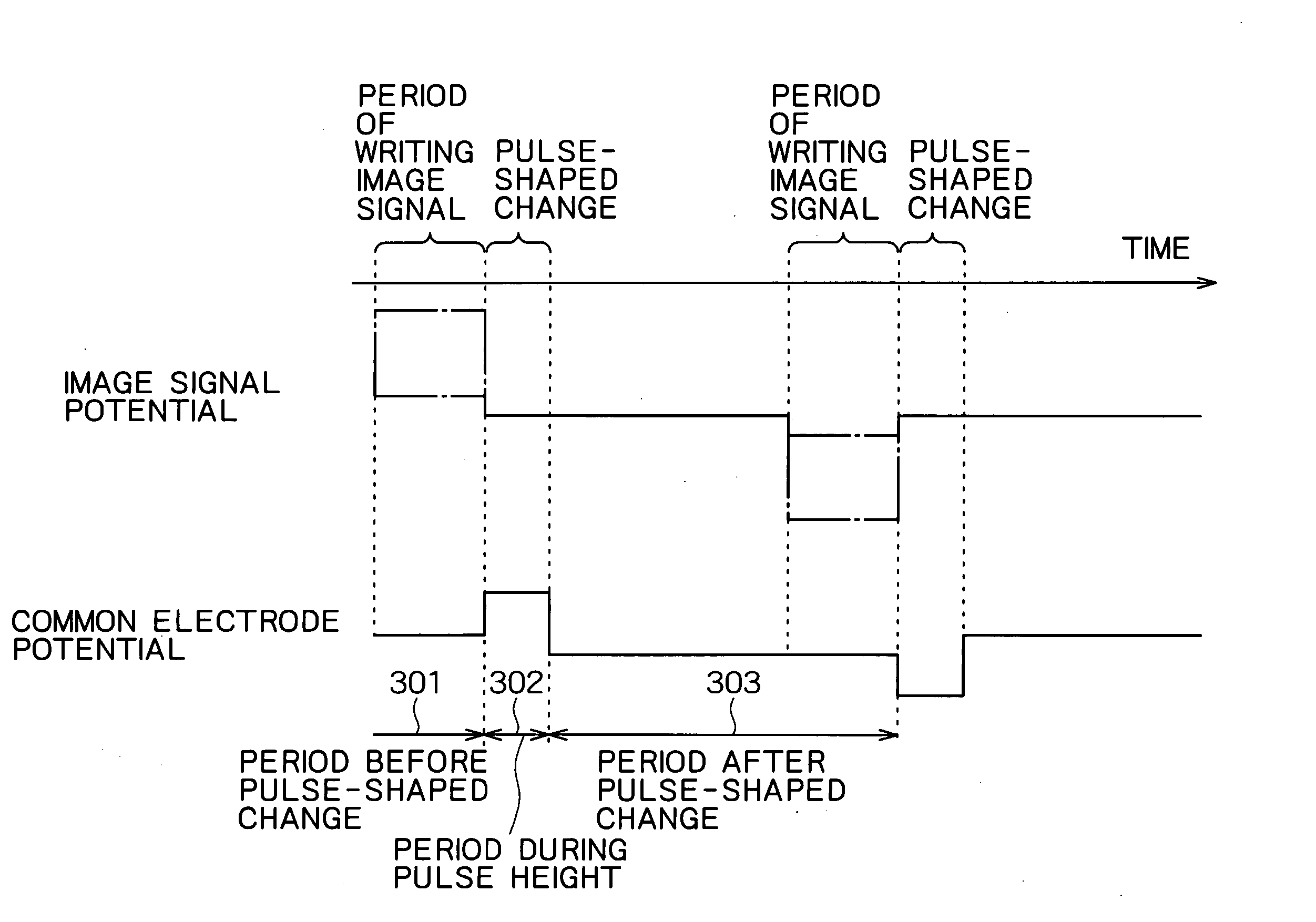
[0163] First, a first embodiment of the present invention will be described with reference to FIGS. 7 and 8. A liquid crystal display device according to this embodiment comprises a display section 200, an image signal drive circuit 201, a scan signal drive circuit 202, a common electrode potential control circuit 203, and a synchronous circuit 204. The display section 200 comprises scan electrodes 212, image signal electrodes 211, a plurality of pixel electrodes 214 arranged in a matrix, a plurality of switching elements 213 for transmitting an image signal to the pixel electrodes 214, and a common electrode 215. The common electrode potential control circuit 203 changes the electric potential of the common electrode 215 into a pulse shape, after the scan signal drive circuit 202 has scanned all the scan electrodes 212 and the image signal has been transmitted to the pixel electrodes 214.
[0164] Then, the operation of the liquid crystal display device according to this embodiment s...
Example
[0166] Next, a second embodiment of the present invention will be described with reference to FIGS. 9 and 10. A liquid crystal display device according to this embodiment comprises a display section 200, an image signal drive circuit 201, a scan signal drive circuit 202, a storage capacitor electrode potential control circuit 205, and a synchronous circuit 204. The display device 200 comprises scan signal electrodes 212, image signal electrodes 211, a plurality of pixel electrodes 214 arranged in a matrix, a plurality of switching elements 213 for transmitting an image signal to the pixel electrodes 214, and a storage capacitor electrode 216. The storage capacitor electrode potential control circuit 205 changes the electric potential of the storage capacitor electrode 216 into a pulse shape, after the scan signal drive circuit 202 has scanned all the scan electrodes 212 and the image signal has been transmitted to the pixel electrodes 214.
[0167] Then, the operation of this embodime...
Example
[0168] Next, a third embodiment of the present invention will be described with reference to FIGS. 11 and 12. A liquid crystal display device according to this embodiment comprises a display section 200, an image signal drive circuit 201, a scan signal drive circuit 202, a common electrode potential control circuit 203, a storage capacitor electrode potential control circuit 205, and a synchronous circuit 204. The display device 200 comprises scan signal electrodes 212, image signal electrodes 211, a plurality of pixel electrodes 214 arranged in a matrix, a plurality of switching elements 213 for transmitting an image signal to the pixel electrodes 214, a common electrode 215 and a storage capacitor electrode 216. The common electrode potential control circuit 203 changes the electric potential of the common electrode 216 into a pulse shape, after the scan signal drive circuit 202 has scanned all the scan electrodes 212 and the image signal has been transmitted to the pixel electrod...
PUM
 Abstract
Description
Claims
Application Information