Three-level leadframe for no-lead packages

a leadframe and no-lead technology, applied in the direction of semiconductor devices, semiconductor/solid-state device details, electrical apparatus, etc., can solve the problems of high cost and no-lead package based on wire bonding technology

Active Publication Date: 2005-07-14
TEXAS INSTR INC
View PDF2 Cites 84 Cited by
  • Summary
  • Abstract
  • Description
  • Claims
  • Application Information

AI Technical Summary

Benefits of technology

[0010] It is further a technical advantage of the invention that the second plurality of leadframe segments has the narrow end portions terminate in the third horizontal plane, remote from the second horizontal plane, in which the wide end portions of the first leadframe plurality are located. This feature allows a tighter segment pitch than would be feasible with an arrangement, in which all segment ends terminate in the same plane. The embodiments of the invention can thus not only accommodate low I / O counts (for example, 8 to about 100), but also intermediate I / O counts (for example, up to 200).

Problems solved by technology

When the flip-chip technology is used in the assembly of semiconductor devices, in spite of its frequently higher cost compared to wire bonding, it is often required in order to meet demanding performance goals.
Most often, however, no-lead packages are based on wire bonding technology.
Only recently have no-lead packages been proposed in the literature for flip-chip assembly; these packages are, however, only suitable for low I / O count (8 to 100 I / O's).

Method used


Image

  • Three-level leadframe for no-lead packages
  • Three-level leadframe for no-lead packages
  • Three-level leadframe for no-lead packages

Examples


Embodiment Construction

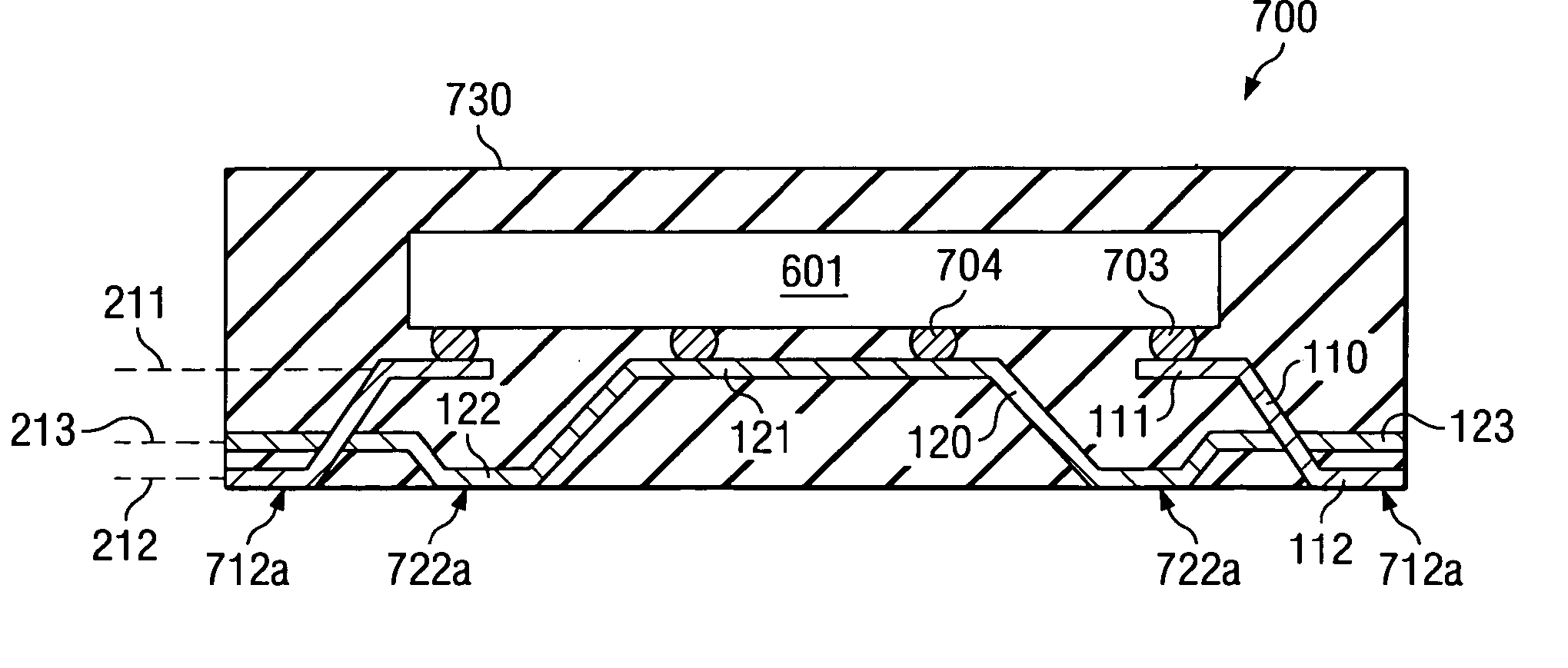
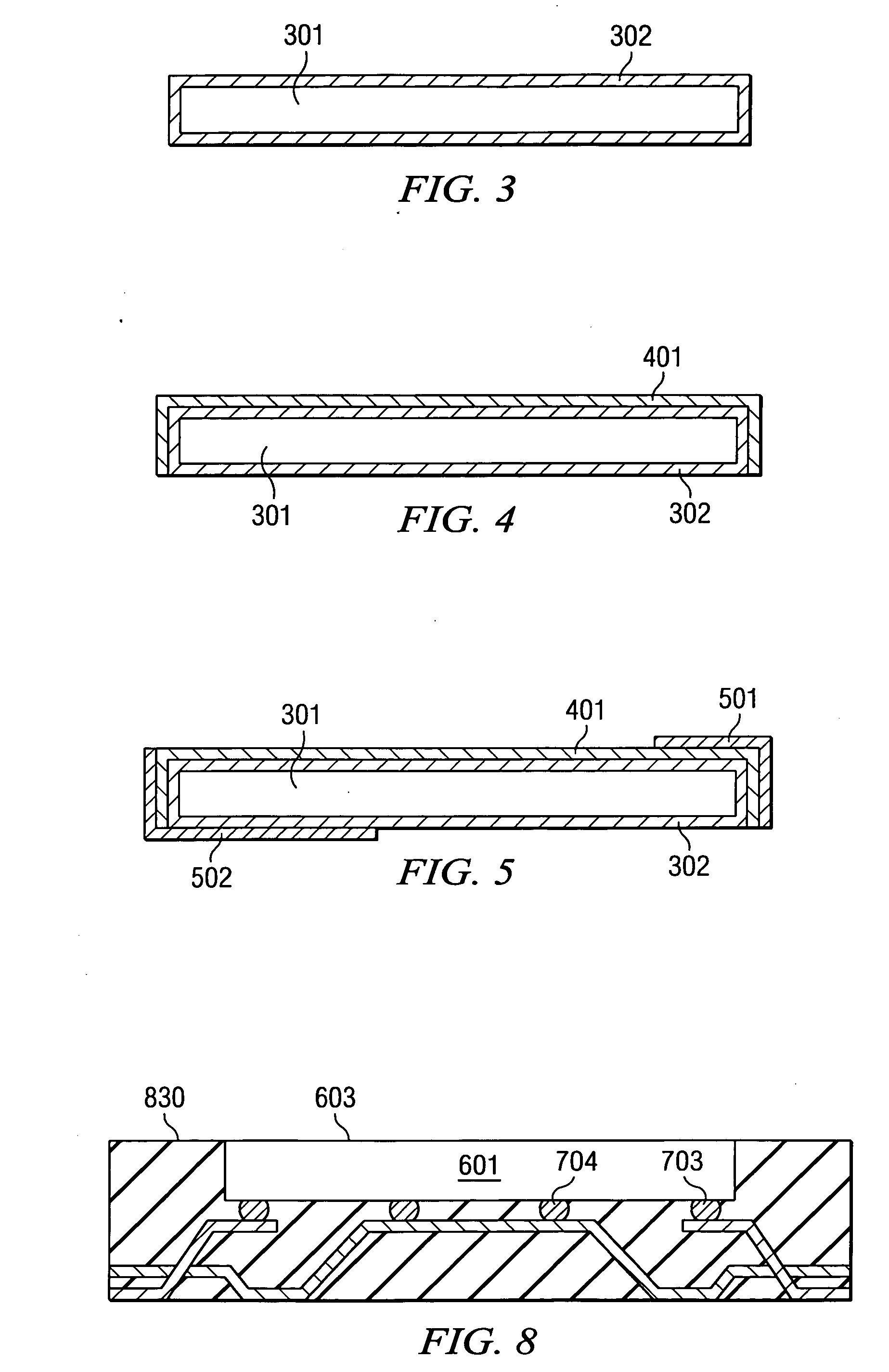
[0020] The present invention is related to U.S. Pat. No. 6,072,230, issued on Jun. 6, 2000 (Carter et al., “Exposed Leadframe for Semiconductor Packages and Bend Forming Method of Fabrication”), and U.S. patent applications Ser. No. 09 / 900,080, filed on Jul. 6, 2001 (Abbott et al., “Preplating of Semiconductor Small Outline No-Lead Leadframes”), and Ser. No. 10 / 346,899, filed on Jan. 17, 2003 (Abbott, “Semiconductor Device with Double Nickel-Plated Leadframe”).

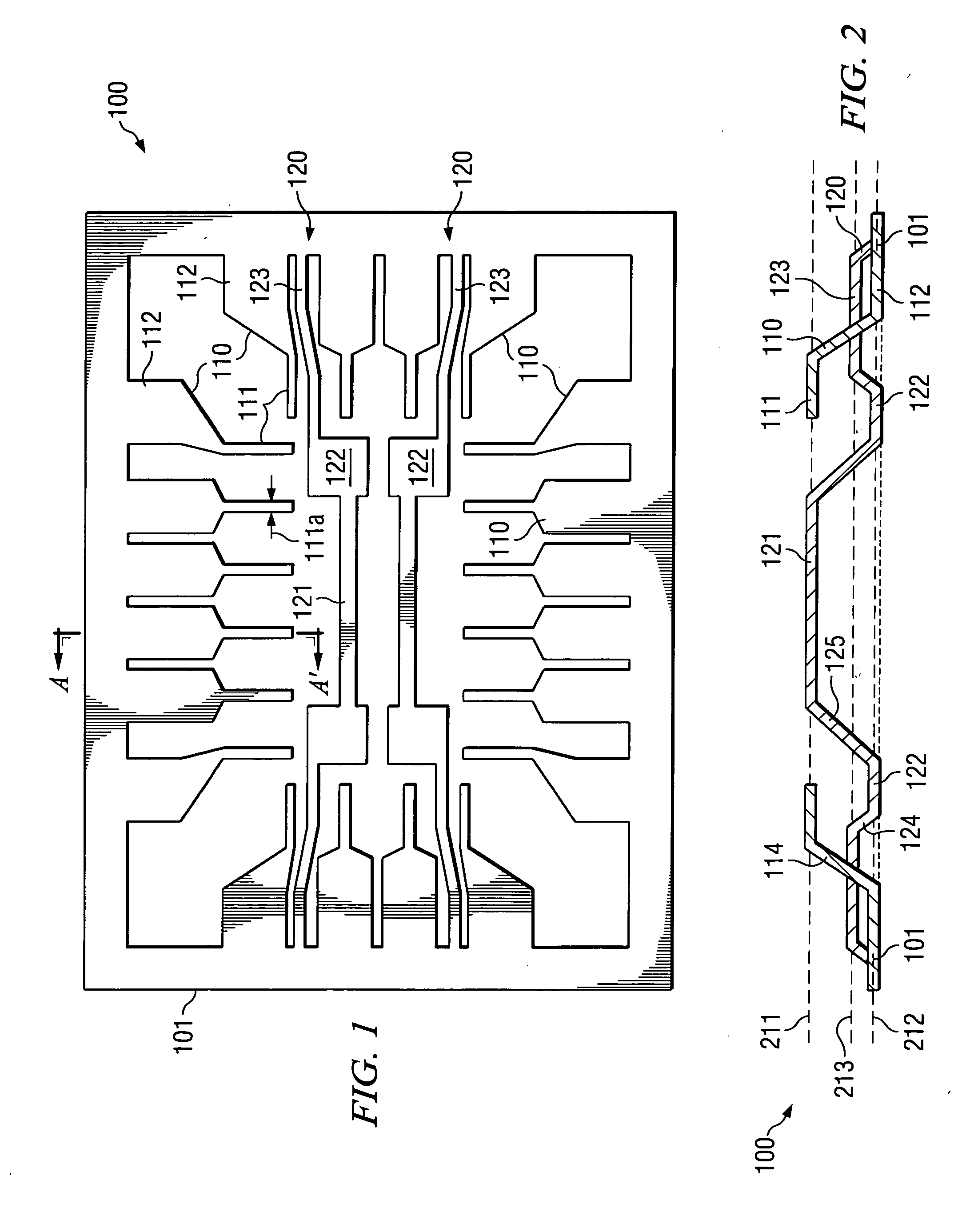
[0021]FIG. 1 is a schematic and simplified top view of a leadframe, generally designated 100, for use in the assembly of semiconductor chips; FIG. 2 is a schematic x-ray view of leadframe 100 after the forming step. FIGS. 1 and 2 illustrate two pluralities of leadframe segments, held together by frame 101. Several segments of the first plurality are designated 110, and several segments of the second plurality are designated 120.

[0022] Each segment 110 of the first plurality has a narrow end portion 111 in a first horizontal ...


PUM


Abstract

A semiconductor device (700) having a leadframe with a first plurality of segments (110) having a narrow end portion (111) in a first horizontal plane (211) and a wide end portion (112) in a second horizontal plane (212). The leadframe further includes a second plurality of segments (120) having a narrow center portion (121) in the first horizontal plane, at least one wide center portion (122) in the second horizontal plane, and narrow end portions (123) in a third horizontal plane (213), which is located between the first and second planes.

Description

FIELD OF THE INVENTION [0001] The present invention is related in general to the field of semiconductor devices and processes, and more specifically to the structure and material of leadframes for integrated circuit devices. DESCRIPTION OF THE RELATED ART [0002] When the flip-chip technology is used in the assembly of semiconductor devices, in spite of its frequently higher cost compared to wire bonding, it is often required in order to meet demanding performance goals. Among these performance goals are higher numbers of input / output (I / O) terminals, shorter electrical paths for higher speed and frequency, and lower heat dissipation paths for improved thermal performance. These performance goals are driven, for instance, by the pervasive growth of semiconductor products for the wireless and computer peripheral markets. Devices with a need for high frequency performance yet low I / O count include power amplifiers and optical transceivers. [0003] In another trend in the semiconductor i...

Claims


Application Information

Patent Timeline
Patent Type & Authority Applications(United States)
IPC IPC(8): H01L23/48H01L23/495
CPCH01L23/4951H01L23/49541H01L23/49551H01L23/49582H01L2224/16H01L2224/16245H01L2924/01078H01L2924/01079H01L2924/00014H01L2924/01046H01L2224/45099
Inventor YAMUNAN, VINU
Owner TEXAS INSTR INC
Why Eureka
Try Eureka