Bias-independent capacitor based on superposition of nonlinear capacitors for analog/RF circuit applications

a capacitor and bias-independent technology, applied in the field of capacitors, can solve the problems of bias-voltage-independent capacitors, fringe capacitors (made by sidewalling of metal lines), mim (metal-insulator-metal) capacitors, poly-oxide-poly capacitors, etc., and achieve the effects of reducing manufacturing costs, increasing manufacturing costs, and increasing manufacturing costs

Inactive Publication Date: 2005-07-21
AVAGO TECH WIRELESS IP SINGAPORE PTE
View PDF1 Cites 5 Cited by
  • Summary
  • Abstract
  • Description
  • Claims
  • Application Information

AI Technical Summary

Benefits of technology

[0006] The present invention is directed to a bias-independent capacitor based on superposition of nonlinear capacitors for

Problems solved by technology

However, the bias-voltage-independent capacitors, such as fringe capacitors (made by sidewalling of metal lines), MIM (metal-insulator-metal) capacitors, or poly-oxide-poly capacitors are fairly expensive.
These types of capacitors require a l

Method used


Image

  • Bias-independent capacitor based on superposition of nonlinear capacitors for analog/RF circuit applications
  • Bias-independent capacitor based on superposition of nonlinear capacitors for analog/RF circuit applications
  • Bias-independent capacitor based on superposition of nonlinear capacitors for analog/RF circuit applications

Examples


Embodiment Construction

[0022] Reference will now be made in detail to the embodiments of the present invention, examples of which are illustrated in the accompanying drawings.

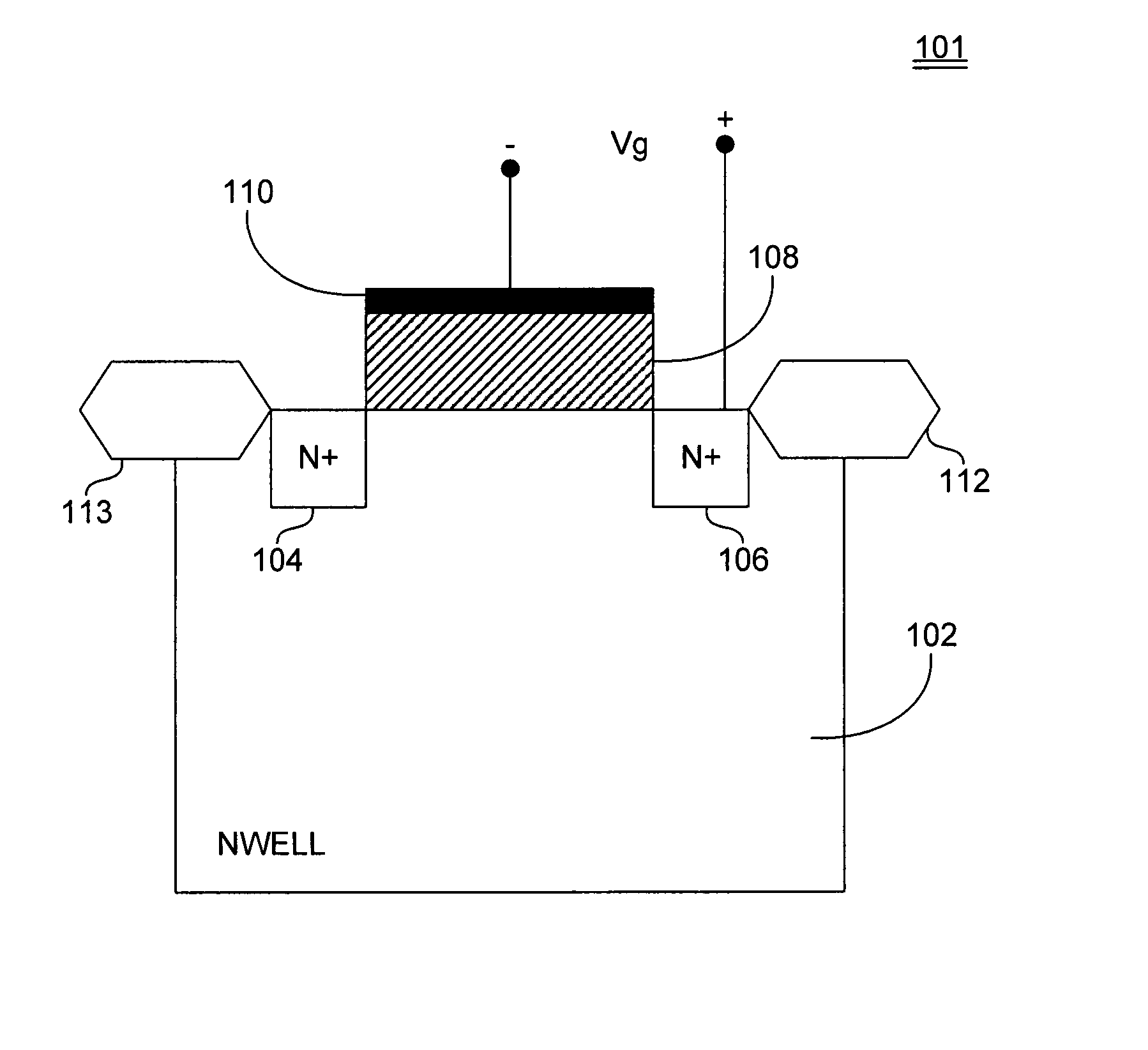
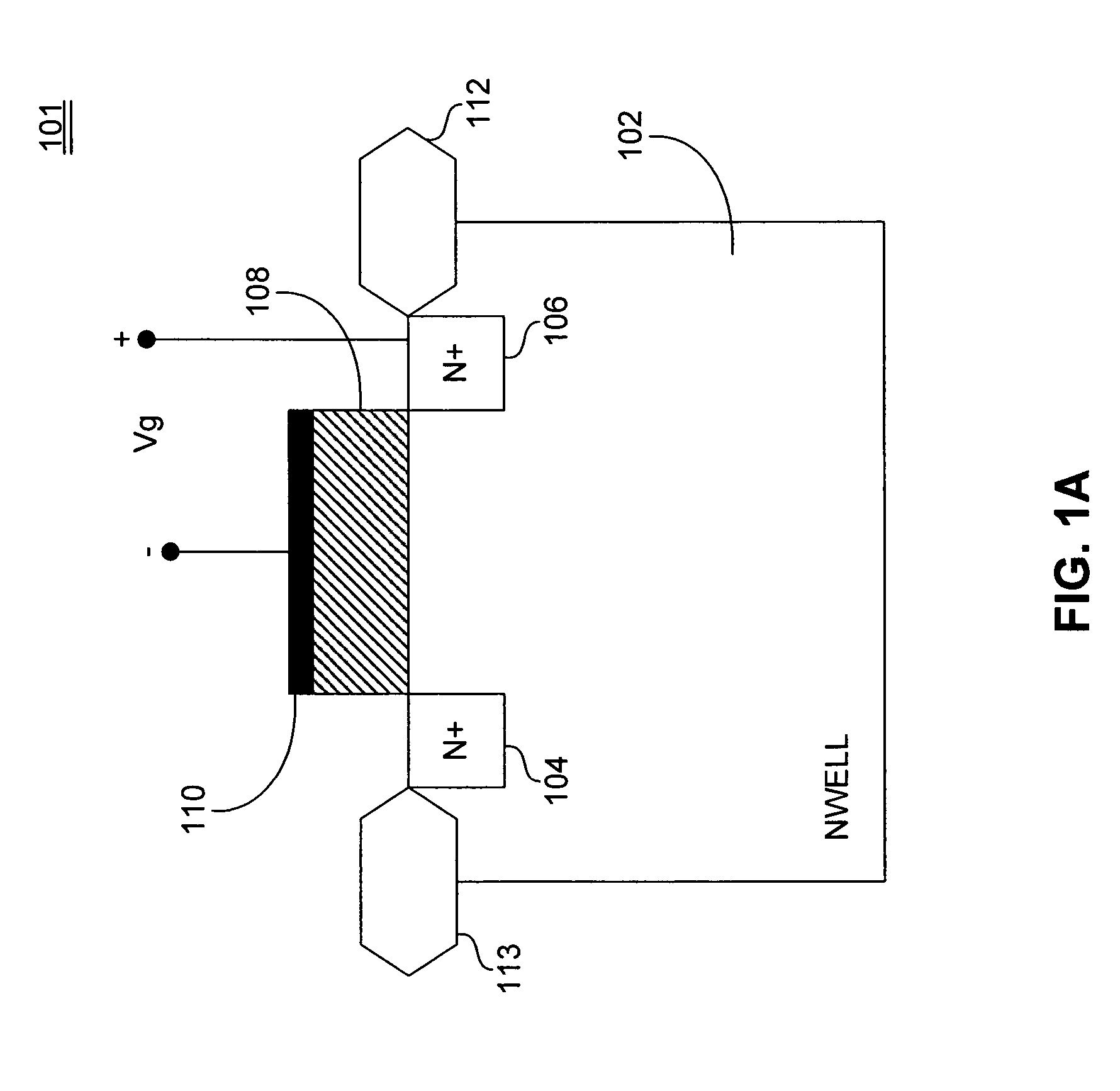
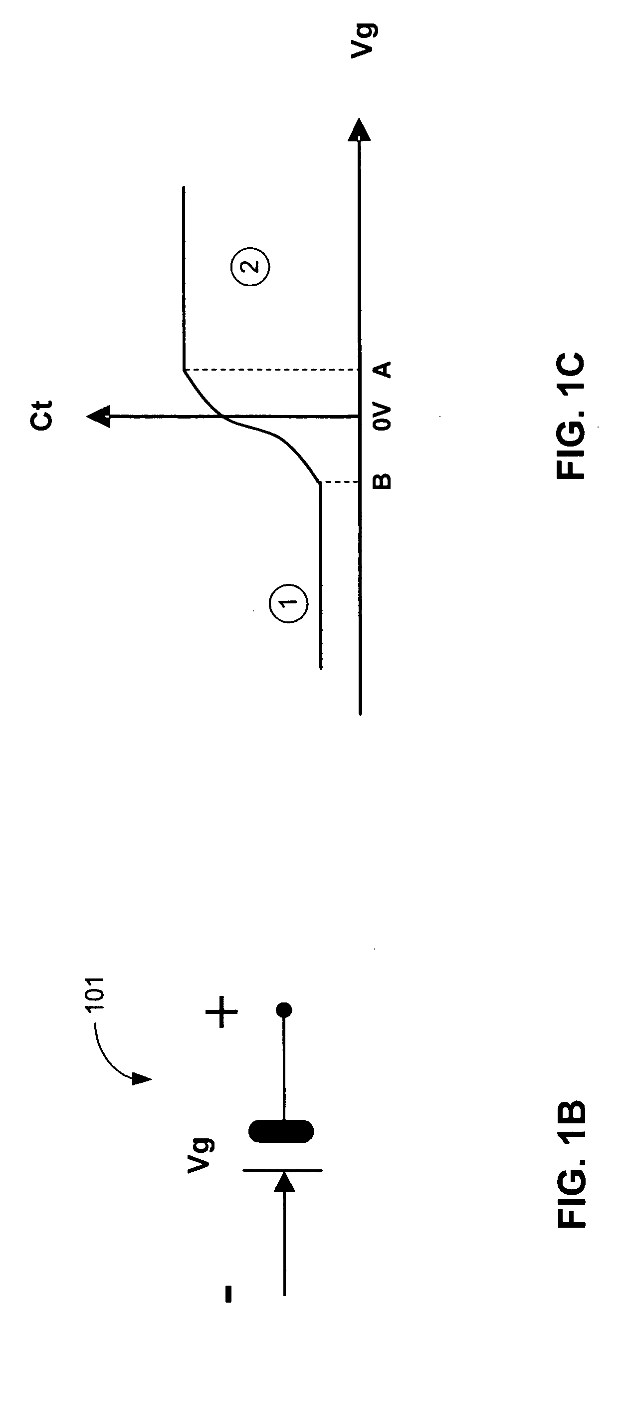
[0023] In this invention, a new method is proposed, based on MOSFET devices, of achieving a high density of capacitance with low-bias dependence and high linearity. For parallel-connected bias-dependent capacitors (such as MOSFET devices) with bias voltage Vg, the total capacitance is Ct(Vg)=Σ Ci(Vg), where each Ci is a function of bias voltage that is applied to both ends. In CMOS technology, for example, a capacitor can be made with NMOS devices, PMOS devices, native-NMOS devices, MOS on NWELL devices, MOS on PWELL devices, or any other capacitor available in that process.

[0024] To achieve a higher density of capacitors in an integrated circuit (IC) chip, MOS devices whose capacitance is based on a thin gate oxide, are the best choice. However, the MOS capacitors are highly bias-voltage dependent, which is not desirable in most a...


PUM


Abstract

A first MOS-on-NWELL device is formed on a substrate and has its pickup terminals optionally connected together. A second MOS-on-NWELL device is formed on the substrate and has its pickup terminals optionally connected together. A gate of the first MOS-on-NWELL device is connected to the pickup terminals of the second MOS-on-NWELL device. A gate of the second MOS-on-NWELL device is connected to the pickup terminals of the first MOS-on-NWELL device. A first PMOS transistor is formed on a substrate and has its source and drain terminals connected together. A second PMOS transistor is formed on a substrate and has its source and drain terminals connected together. A gate of the first PMOS transistor is connected to the source and drain terminals of the second PMOS transistor. A gate of the second PMOS transistor is connected to the source and drain terminals of the first PMOS transistor. A combination of the first and second PMOS transistors are connected in parallel with the first and second MOS-on-NWELL devices.

Description

BACKGROUND OF THE INVENTION [0001] 1. Field of the Invention [0002] The present invention is related to capacitors used in integrated circuits, and more particularly, to linear capacitors for use in analog and RF circuits. [0003] 2. Related Art [0004] In analog / RF integrated circuits, bias-voltage-independent capacitors are needed to achieve high linearity of circuit performance. However, the bias-voltage-independent capacitors, such as fringe capacitors (made by sidewalling of metal lines), MIM (metal-insulator-metal) capacitors, or poly-oxide-poly capacitors are fairly expensive. These types of capacitors require a large surface area or additional processing steps, leading to higher manufacturing costs. On the other hand, MOSFET-type capacitors have the highest capacitance per unit area, since they are formed by thin gate-oxide, but their capacitance value is dependent on the gate / pickup terminals voltage, and is often non-linear. [0005] Traditionally, circuit designers have chose...

Claims


Application Information

Patent Timeline
IPC IPC(8): H01L27/108H01L29/78
CPCH01L29/78
Inventor CHEN, CHUN-YINGSONG, JUNGWOO
Owner AVAGO TECH WIRELESS IP SINGAPORE PTE
Why Eureka
Try Eureka