

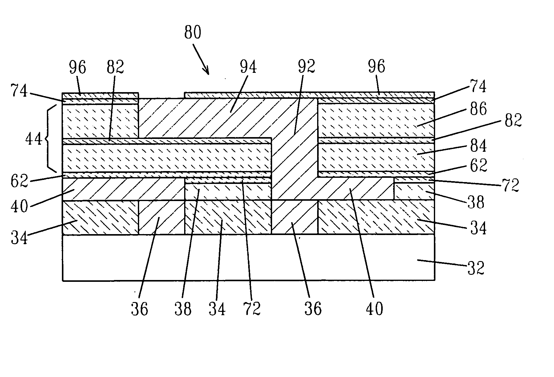
Low k and ultra low k SiCOH dielectric films and methods to form the same
a dielectric film, ultra-low k technology, applied in the direction of chemical vapor deposition coating, semiconductor/solid-state device details, coatings, etc., can solve the problems of cracks, chip formation, and inability to stabilize sicoh films
- Summary
- Abstract
- Description
- Claims
- Application Information
AI Technical Summary
Benefits of technology
Problems solved by technology
Method used
Image

Examples
process embodiments
First Implementation Example, k=2.7
[0079] In a preferred process embodiment, a 300 mm substrate is placed in a PECVD tool on a heated wafer chuck at 300°-425° C. and preferably at 350° C. Any PECVD deposition reactor may be used in the present invention. Gas and liquid precursor flows are then stabilized to reach a pressure of 6 torr, although pressures from 1-10 torr may be used.
[0080] The gas composition consists of He or Ar, a SiCOH precursor, and optionally O2 or CO2. The SiCOH precursor contains the elements Si, C, O and H and preferred precursors include tetramethylcyclotetrasiloxane (TMCTS) or octamethylcyclotetrasiloxane (OMCTS), diethoxymethylsilane (DEMS), dimethyldimethyoxysilane (DMDMOS), diethyldimethoxysilane (DEDMOS) and related cyclic and non-cyclic silanes, siloxanes and the like. The preferred process uses octamethylcyclotetrasiloxane (OMCTS) at liquid flow of 2000-3500 mg / minute (preferably 2800±300 mg / minute) and O2 at a flow of 100-200 sccm, although O2 flows ...
second implementation example
, k=2.5 to 2.6
[0088] To make the SiCOH materials of the invention with k=2.5 to 2.6, a process similar to the 1st implementation example is used, but small changes are made. Specifically, the pressure is increased above 6 torr, the SiCOH OMCTS precursor flow is decreased to about 1500-3000 mg / minute, the showerhead RF power is slightly reduced (10-20% reduction). It is important to reduce the wafer chuck RF power by about 20-50%.
third implementation example
, k=2.4 to 2.2
[0089] In a preferred process embodiment, a 300 mm substrate is placed in a PECVD tool on a heated wafer chuck at 100-400° C. and preferably at 200°-350° C. Tools such as the Producer made by Applied Materials and the Vector made by Novellus Systems are commonly used, although any PECVD deposition reactor may be used within the invention.
[0090] Gas and liquid precursor flows are then stabilized to reach a pressure of 1 to 6 torr, although pressures from 0.1-10 torr may be used. The gas composition consists of a SiCOH precursor, a 2nd hydrocarbon based precursor and He or Ar. Optionally, O2 or CO2 is also used. The SiCOH precursor contains the elements Si, C, O and H and preferred precursors include tetramethylcyclotetrasiloxane (TMCTS) or octamethylcyclotetrasiloxane (OMCTS), diethoxymethylsilane (DEMS), dimethyldimethoxysilane (DMDMOS), diethyldimethoxysilane (DEDMOS) and related cyclic and non-cyclic silanes, siloxanes and the like.
[0091] Processes described in U.S...
PUM
| Property | Measurement | Unit |
|---|---|---|
| Temperature | aaaaa | aaaaa |
| Thickness | aaaaa | aaaaa |
| Thickness | aaaaa | aaaaa |
Abstract
Description
Claims
Application Information