

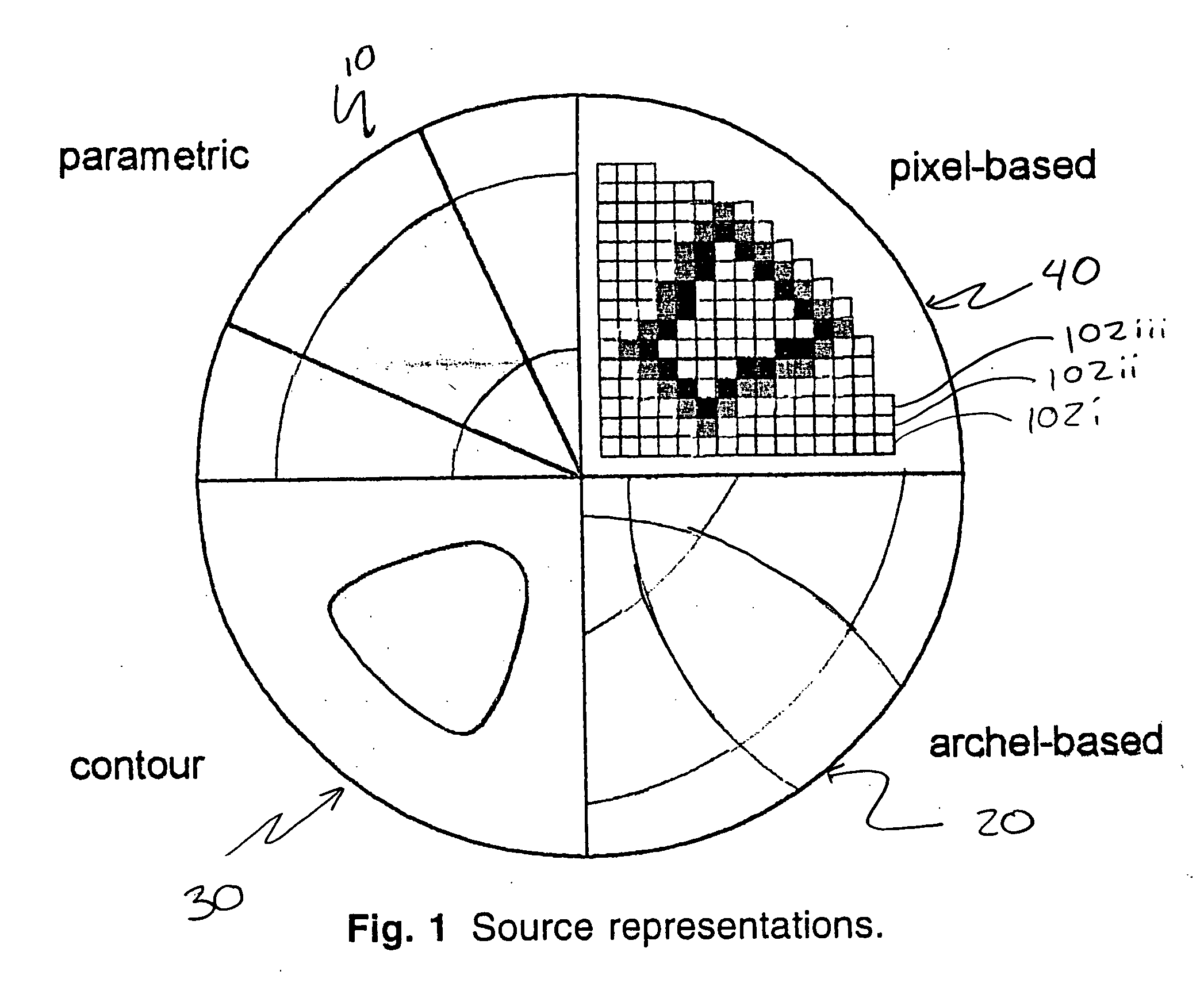
Source optimization for image fidelity and throughput
a source optimization and image fidelity technology, applied in the field of photolithographic processing techniques, can solve the problems of not being able to reliably determine the practical optimum illumination pattern for a given layout pattern, affecting the performance of the circuit, and forming very complex source shapes
- Summary
- Abstract
- Description
- Claims
- Application Information
AI Technical Summary
Benefits of technology
Problems solved by technology
Method used
Image

Examples
example 1
Periodic Array of Contacts, Alternating PSM
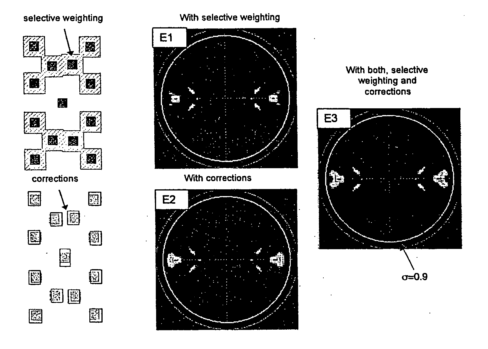
[0083] Geometries and process conditions for our first two examples are borrowed from the Burkhardt paper. Contact patterns A and B are shown in FIG. 7. They are composed of clear and 180° phase shifted, 210 nm contact holes that are imaged on a dark background using λ=248 nm and NA=0.5. Contact pattern A has 640 nm pitch in the γ and 320 nm pitch in the x direction. Contact pattern B is less regular, with a basic pitch of 320 nm in both directions. Pupil diagrams are shown in the second column of FIG. 7. Positions of diffraction orders are marked by small squares, with their brightness being proportional to the order amplitudes. Thick white circles show the source area σ=0.6.
[0084] For the pattern A, four light squares represent the major diffraction orders that are larger than the four minor diffraction orders, marked as the darker squares and positioned farther from the x-axis. Around each of the eight shown diffraction orders a unit c...
example 2
SRAM Design 1, Binary Mask
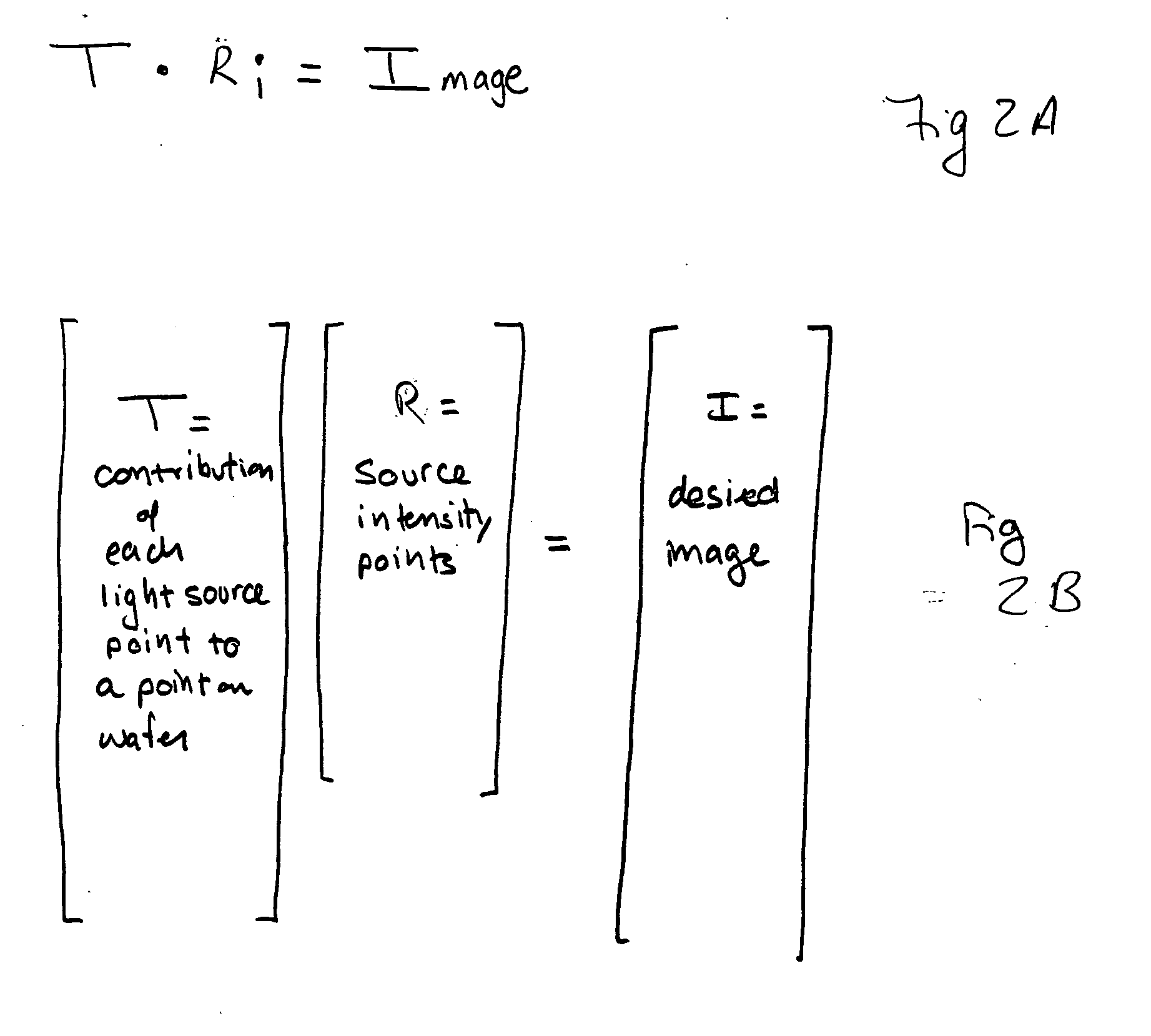
[0087] In this section we consider a 130 nm SRAM design from the Brist paper. Geometry of this SRAM cell is much more complicated than for the contacts from the previous section and cannot be tackled by a simple analysis of diffraction orders. The cell from FIG. 9 tiles large region of the SRAM design in a way that is called in geometry wallpapers tiling group pmm. A fundamental cell of this tiling consists of four mirrored patterns of FIG. 9, with symmetries along the vertical and horizontal axis. These symmetries reduce the solution of the optimization problem to one quadrant of the source, with subsequential mirroring of results along vertical and horizontal axes. Simulation runtime can be reduced farther by simulating one-forth of the fundamental cell, then filtering its spectrum to induce even periodic boundary conditions in both the vertical and horizontal directions. The optimization domain is chosen to be a circle of σ=0.8 and the balancing paramet...
example 3
SRAM Design 2, Attenuated Mask
[0089] In this example the SRAM pattern and process conditions are similar to the Barouch paper. We optimize the source for the SRAM cell shown in FIG. 13 with the purpose of comparing contour-based, as in the Barouch paper, and pixel-based optimization results. A uniform weighting style is chosen with the weight 32, balance parameter γ is 0.38, and optical conditions are λ=248 nm, NA=0.5, σ=0.8.
[0090] Optimizations were run for the scaled designs with 140 nm, 160 nm, 180 nm, 200 nm, 220 nm, and 250 nm feature sizes. The resulting source configurations D1, D2, . . . , D6 are shown in FIG. 9 as contours of 0.25 intensity levels. For the 250 nm design, the source D6 is a combination of the diagonal quadrapole and a weak vertical dipole. This configuration is different from the one found in the Barouch paper, which looks like an annulus of 0.6 and 0.72 radii. Simulations along the horizontal cutline a-a through the center of the cell show potential super...
PUM
 Abstract
Description
Claims
Application Information