Complementary replacement of material

a technology of composite materials and etching steps, applied in semiconductor devices, solid-state devices, decorative arts, etc., can solve the problems of reducing the ability of resists to serve as etch masks for subsequent etch steps, increasing the difficulty of patterning and etching steps, and requiring a higher degree of control, so as to achieve high contrast resist lines and reduce the effect of etching steps

Inactive Publication Date: 2008-07-15
TAIWAN SEMICON MFG CO LTD
View PDF15 Cites 16 Cited by
  • Summary
  • Abstract
  • Description
  • Claims
  • Application Information

AI Technical Summary

Benefits of technology

[0017]In a second embodiment, a via hole pattern in a damascene stack comprised of a top dielectric layer and a bottom etch stop layer is provided on a substrate. A resist is coated on the dielectric layer and is patterned by using a phase edge mask to give a high contrast resist line with large DOF. The line occupies a region over the via holes that will become a trench in the damascene structure. A CMR layer similar to the one described in the first embodiment is coated over the patterned resist. An etch is performed which removes the patterned resist at a faster rate than the CMR layer. As a result, a trench opening is formed in the CMR layer and this opening can be transferred into the dielectric layer in a subsequent etch step. The CMR layer is stripped and the dual damascene structure is completed by a conventional process sequence. Smooth edges on the CMR pattern minimize roughness on the sidewalls of the trench opening in the dielectric layer. A thinner photoresist layer can be coated that will enable a larger process window. Additionally, the photoresist that fills the via is not removed by developer and avoids scumming and poisoning problems tha

Problems solved by technology

As the size of circuits shrinks in order to keep pace with demand for higher performance, the patterning and etching steps become more difficult and require a higher degree of control.
Unfortunately, as higher resolution resists have been developed for shorter exposing wavelengths, the etch resistance of the polymer component has decreased and the capability of the resist to serve as an etch mask for a subsequent etch step has diminished.
However, for sub-200 nm exposure wavelengths like 193 nm, aromatic polymers are not useful because of a high optical absorbance.
Although COMA copolymers are better than acrylat

Method used


Image

  • Complementary replacement of material
  • Complementary replacement of material
  • Complementary replacement of material

Examples


first embodiment

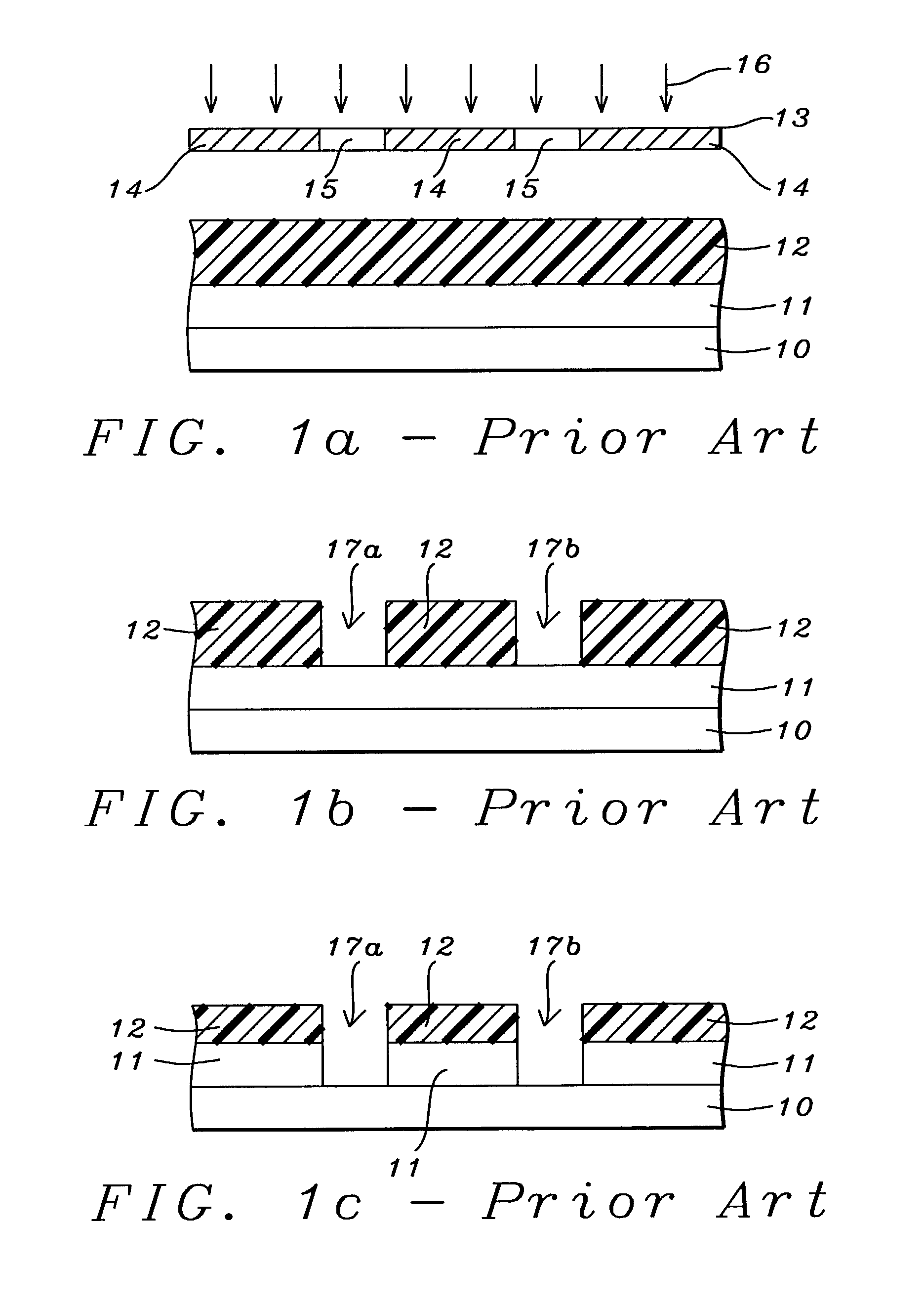
[0030]FIGS. 2a-2e are drawings showing a method of forming a pattern with high resolution contact holes and transferring the pattern into an underlying layer according to the present invention. Referring to FIG. 2a, a dielectric layer 21 is formed on substrate 20. Substrate 20 may contain conducting layers and other dielectric layers (not shown). Dielectric layer 21 is typically SiO2 or a low k dielectric material such as fluorine doped SiO2, carbon doped SiO2, fluorosilicate glass (FSG) or Applied Materials' “Black Diamond” that is deposited with a CVD or plasma enhanced CVD (PECVD) technique. Optionally, commercially available spin-on dielectrics such as FLARE from Allied Signal and SiLK from Novellus can be used.

[0031]A resist solution is coated and baked to form layer 22. Resist 22 is preferably a positive tone composition. In a positive tone resist, exposed regions become soluble in a developer and are washed away while unexposed regions remain on the substrate. With a negative...

second embodiment

[0042]In a second embodiment the present invention is a method of forming high resolution polysilicon gates with smooth sidewalls as illustrated in FIGS. 7a-7d. A substrate 70 is provided in FIG. 7a that is comprised of a material such as silicon that contains active regions separated by isolation regions (not shown). A gate dielectric layer that normally consists of SiO2 which is grown on active regions is not shown in order to simplify the drawing and focus attention on the key features of the present embodiment. A polysilicon layer 71 is deposited by conventional means such as a CVD technique. Optionally, an anti-reflective coating (ARC) which is not shown is coated on the polysilicon 71 to control reflectivity during a subsequent patterning step. A resist solution is coated on the polysilicon layer 71 and baked to form resist layer 72.

[0043]The resist 72 is exposed with radiation 76 comprised of one or more wavelengths in the range of about 13 nm to about 500 nm through mask 73....

third embodiment

[0049]In a third embodiment the present invention is a method of forming trenches such as in a via first dual damascene process as depicted in FIGS. 8a-8d. A substrate 80 is provided in FIG. 8a that is comprised of dielectric and conducting layers (not shown). An etch stop layer 81 consisting of a material such as silicon carbide, silicon nitride or silicon oxynitride is deposited by a CVD or PECVD method. A dielectric layer 82 is deposited and via holes 83a and 83b are formed by conventional methods. Although two holes are shown in this example, the via hole pattern in layer 82 can include dense hole regions and isolated hole regions. Dielectric layer 82 is selected from a group including SiO2 and low k dielectric materials such as fluorine doped SiO2, carbon doped SiO2, FSG, and borophosphate silicate glass. Optionally, an etch stop layer (not shown) may be deposited on layer 82 prior to via hole patterning to serve as an etch stop for a subsequent chemical mechanical polish (CMP)...


PUM

PropertyMeasurementUnit
Wavelengthaaaaaaaaaa
Electrical resistanceaaaaaaaaaa

Abstract

An image reversal method is described that removes the etch resistance requirement from a resist. A high resolution resist pattern comprised of islands, lines, or trenches is formed with a large process window by exposing through one or more masks including phase edge masks and optionally with resolution enhancement techniques. A complementary material replacement (CMR) layer comprised of an organic polymer or material such as fluorosilicate glass which has a lower etch rate than the resist is coated over the resist pattern. CMR and resist layers are etched simultaneously to provide an image reversed pattern in the CMR layer which is etch transferred into a substrate. The method avoids edge roughness like bird's beak defects in the etched pattern and is useful for applications including forming contact holes in dielectric layers, forming polysilicon gates, and forming trenches in a damascene process. It is also valuable for direct write methods where an image reversal scheme is desired.

Description

FIELD OF THE INVENTION[0001]The invention relates to the field of fabricating semiconductor devices and other electronic devices, and more particularly to an image reversal method of forming high resolution lithographic patterns that have high etch resistance.BACKGROUND OF THE INVENTION[0002]Two important processes that are repeated frequently during the manufacture of integrated circuits are photoresist patterning and etch transfer of the pattern into an underlying substrate. As the size of circuits shrinks in order to keep pace with demand for higher performance, the patterning and etching steps become more difficult and require a higher degree of control.[0003]To achieve a higher resolution pattern in a photoresist, hereafter referred to as resist, the exposing wavelength has decreased according to an improvement predicted by the Raleigh equation, R=kλ / NA where R is the resolution of a feature printed in a lithographic process, k is a process constant, λ is the wavelength of radi...

Claims


Application Information

Patent Timeline
IPC IPC(8): H01L21/302
CPCH01L21/0271H01L21/0332H01L21/0337H01L21/32139H01L21/76802H01L21/76808H01L21/31144H01L2221/1026
Inventor LIN, BURN-JENGLIN, HUA-TAILIU, RU-GUNGAU, TSAI-SHENGHO, BANG-CHIEN
Owner TAIWAN SEMICON MFG CO LTD
Why Eureka
Try Eureka