Long range corrections in integrated circuit layout designs

Active Publication Date: 2005-09-29
SIEMENS PROD LIFECYCLE MANAGEMENT SOFTWARE INC
View PDF28 Cites 15 Cited by
  • Summary
  • Abstract
  • Description
  • Claims
  • Application Information

AI Technical Summary

Problems solved by technology

One source of error that can be mitigated but not eliminated are long range intensity variations such as flare from the photolithographic printing system itself.
Flare is caused by the scattering of illumination lig...

Method used


Image

  • Long range corrections in integrated circuit layout designs
  • Long range corrections in integrated circuit layout designs
  • Long range corrections in integrated circuit layout designs

Examples


Embodiment Construction

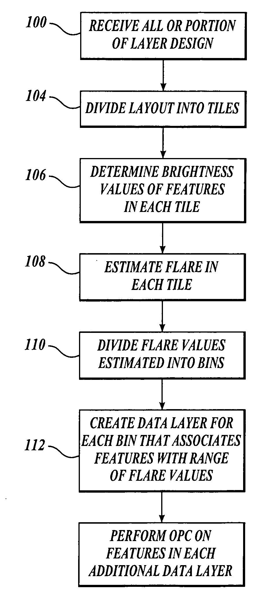
[0013] As indicated above, the present invention is a method for compensating for long range variations such as flare intensity across a layer of an integrated circuit or other device to be created with a photolithographic process.

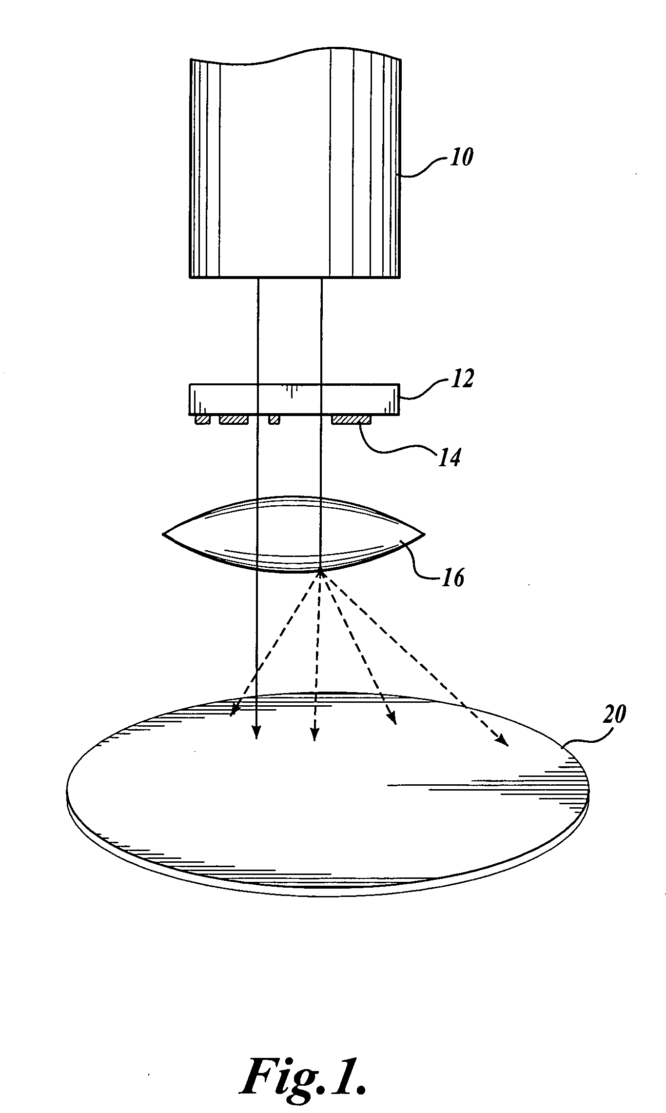
[0014]FIG. 1 is a simplified illustration of a photolithographic imaging system. A light source 10 provides illumination light or electromagnetic energy that is delivered through a mask or reticle 12 that includes a pattern of features 14 to be imaged on a semiconductor wafer 20. Upon exposure of the semiconductor wafer to the illumination light through the mask 12, selective areas of photosensitive chemicals on the wafer are exposed. These exposed areas are then chemically and mechanically processed and polished in order to produce the desired pattern of circuit elements on the wafer.

[0015] If the illumination system were flawless, a single point of light originating from the light source 10 would pass through the mask 12 and a lens system 16 to be dire...


PUM


Abstract

A method and apparatus for compensating for flare intensity variations across an integrated circuit. A layout description for a physical layer of an integrated circuit or portion thereof is divided into a number of regions such as adjacent tiles. An estimate of the flare intensity in each region is determined. The flare intensity values calculated are divided into a number of ranges. In one embodiment, a data layer in a layout description is defined for each range of flare values computed. Features to be printed in an area having a flare value in a particular range are associated with a corresponding additional data layer. The features associated with each additional data layer are analyzed with a resolution enhancement technique that is selected or adjusted to compensate for differing flare values occurring in the integrated circuit.

Description

CROSS-REFERENCES TO RELATED APPLICATIONS [0001] The present application claims the benefit of U.S. Provisional Patent Application No. 60 / 547,484, filed Feb. 25, 2004, which is herein incorporated by reference.FIELD OF THE INVENTION [0002] The present invention relates to resolution enhancement techniques for photolithographic processing and in particular to methods of compensating for long range variations across a layer of an integrated circuit. BACKGROUND OF THE INVENTION [0003] As the number of circuit elements to be created on an integrated circuit continually increases and the size of each element correspondingly decreases, each step in the creation of such circuits via photolithographic processing is analyzed to determine sources of possible processing distortions. For example, it is now common practice for circuit designers to apply one or more resolution enhancement technique (RETs) such as optical and process correction (OPC) that compensate for expected optical distortions...

Claims


Application Information

Patent Timeline
IPC IPC(8): G03F1/00G06F17/50
CPCG03F1/144G06F2217/12G06F17/5068G03F1/70G06F30/39G06F2119/18Y02P90/02
Inventor WORD, JAMESCOBB, NICOLAS B.GRANIK, YURI
Owner SIEMENS PROD LIFECYCLE MANAGEMENT SOFTWARE INC
Why Eureka
Try Eureka