

Dense OPC
a technology of opc and opc, applied in the field of optical and process correction, can solve the problems of inefficient and time-consuming process of estimating how features will print, optical distortion can occur,
- Summary
- Abstract
- Description
- Claims
- Application Information
AI Technical Summary
Problems solved by technology
Method used
Image

Examples
Embodiment Construction
[0023]The present invention is a technique for calculating process conditions in order to perform optical and process correction (OPC) or other resolution enhancement techniques on a target layout design of features to be created on a semiconductor wafer.
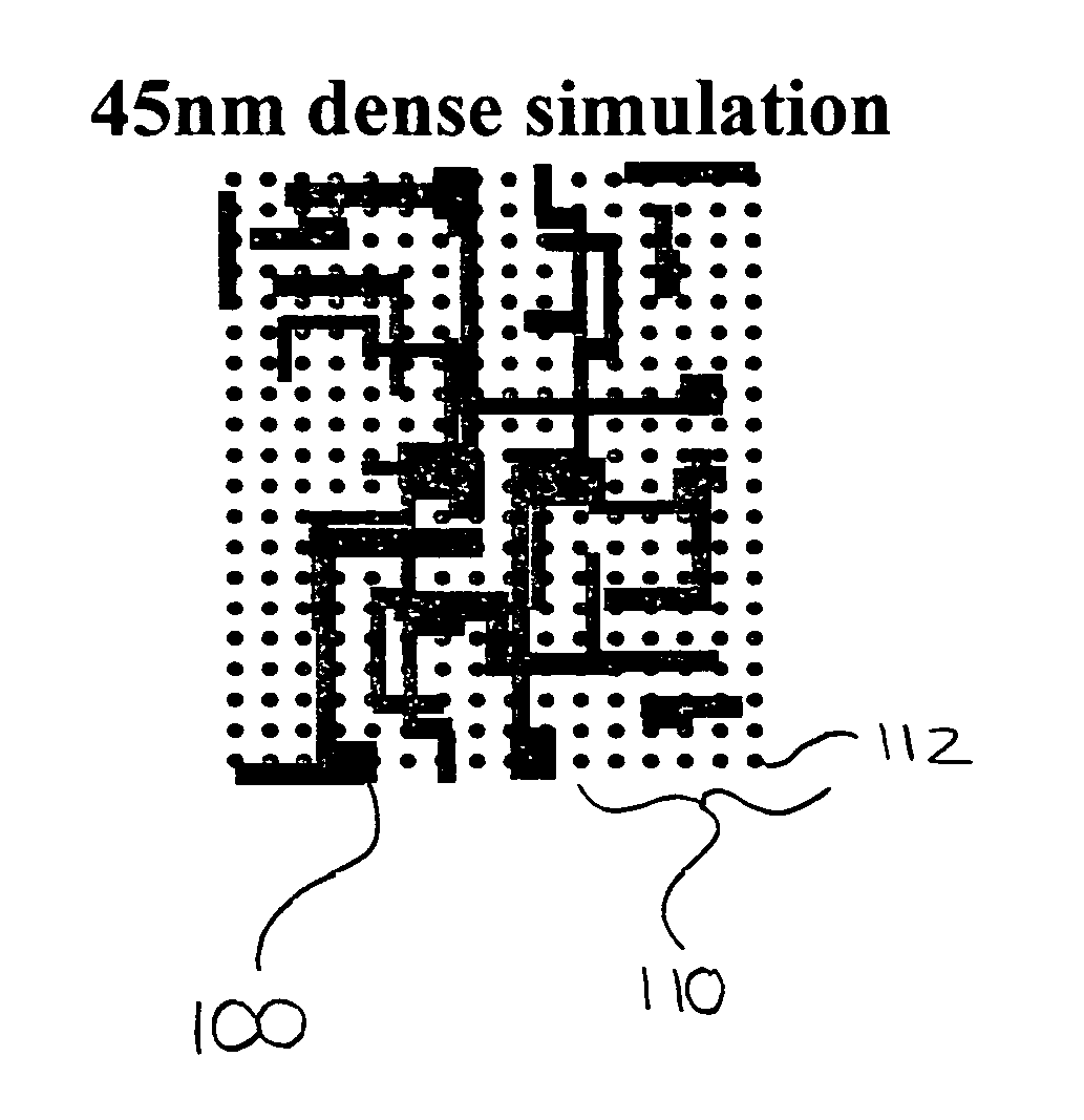
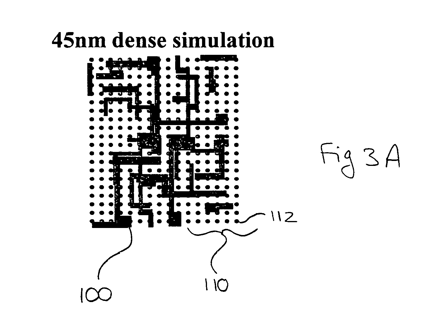
[0024]As shown in FIG. 3A, a target layout design includes a number of features 100 that correspond to circuit elements to be created on a semiconductor wafer. In one embodiment, each feature 100 is defined as a polygon in a standard layout database language such as GDS-II or OASIS™. In order to improve the fidelity by which the pattern of features 100 can be created on a semiconductor wafer, simulations of one or more process conditions are performed on a grid 110 of sample points 112. The grid 110 may be uniform across the entire layout. Alternatively, the grid may have sample points 112 at a wider pitch in areas of the circuit contain fewer features or features that are not critical to circuit operation. Alternatively, those feat...
PUM
 Abstract
Description
Claims
Application Information