Method for verification of resolution enhancement techniques and optical proximity correction in lithography

An optical proximity correction, resolution enhancement technology, applied in the fields of originals for optomechanical processing, optics, special data processing applications, etc., which can solve problems such as inter-stage interactions that are not easy to define or measure

Inactive Publication Date: 2006-05-24
IBM CORP
View PDF0 Cites 15 Cited by
  • Summary
  • Abstract
  • Description
  • Claims
  • Application Information

AI Technical Summary

Problems solved by technology

However, many destructive wafer failures occur on complex two-dimensional shapes, often including interstage interactions that are not easily defined or measured on simulated wafer images

Method used


Image

  • Method for verification of resolution enhancement techniques and optical proximity correction in lithography
  • Method for verification of resolution enhancement techniques and optical proximity correction in lithography
  • Method for verification of resolution enhancement techniques and optical proximity correction in lithography

Examples


Embodiment Construction

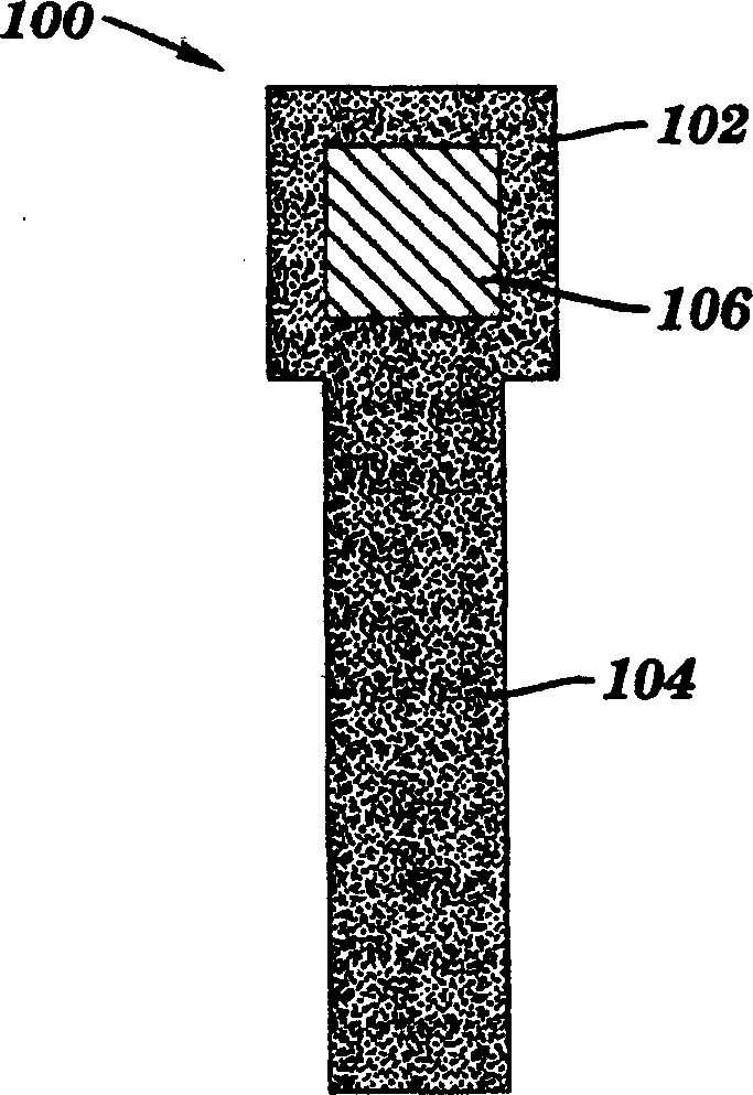
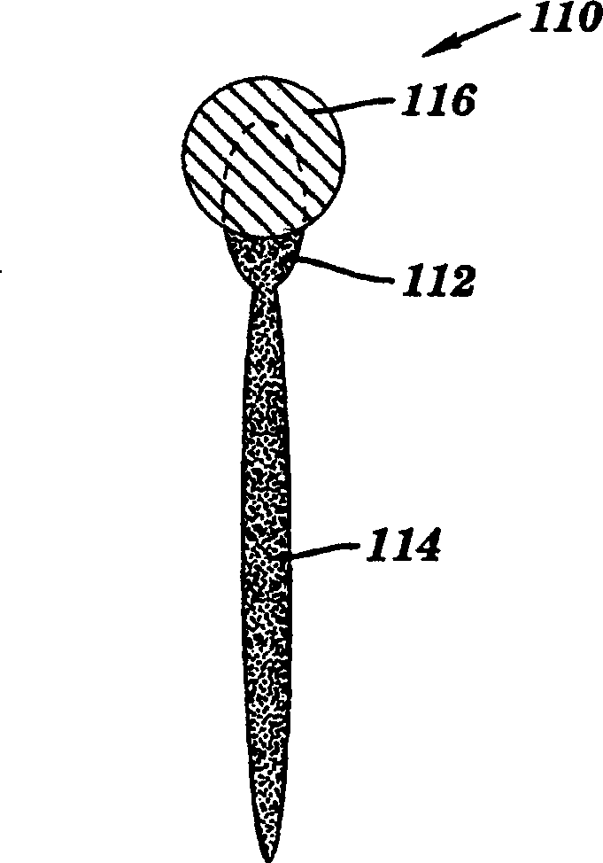
[0020] Referring first to FIG. 1( a ), there is shown a portion of an example integrated circuit layout 100 featuring a polymer conductor (PC) 102 (shown in solid color) and an associated conductive path 104 that communicates with a contact area (CA) 106 (shown as diagonal hatching) together solder the connection to the PC to the previous wiring level. As noted above, when a photolithographic system attempts to print circuit elements whose dimensions are close to the wavelength of the exposing radiation, the shape of the resulting printed circuit element becomes significantly different from the corresponding pattern on the mask. Therefore, to provide qualitative insight into patterning specific layout shapes, simulated wafer images of layout shapes have been enhanced using RET and OPC. FIG. 1( b ) thus shows an example diagram of one possible simulated wafer image 110 of the design layout 100 of FIG. 1( a ). Note that the simulated wafer image 110 shows deformations in the si...


PUM


Abstract

A method for model-based verification of resolution enhancement techniques (RET) and optical proximity correction (OPC) in lithography, the method comprising: scaling the shape of a drawn mask layout to its corresponding intended wafer dimensions to generate a scaled image. The first feature thereof is offset relative to the second feature of the scale image according to a predetermined maximum overlay error. Intersection parameters of said first and said second features of said scale image are calculated to determine a yield measure of an ideal layout. The first feature thereof is offset relative to the second feature of the simulated wafer image according to the predetermined maximum overlay error. calculating an intersection parameter of said first and said second features of said simulated wafer image to determine a yield metric of a simulated layout, and comparing said yield metric of said simulated wafer image to said yield of said scaled image measure.

Description

technical field [0001] The present invention relates generally to semiconductor device fabrication, and more particularly to methods and systems for resolution enhancement techniques and optical proximity correction in verification lithography. Background technique [0002] Fabrication of integrated circuits on semiconductor substrates typically involves a variety of photolithographic steps. The photolithography process begins by applying a thin layer of photoresist material on the substrate surface. The photoresist is then exposed to a radiation source by a lithographic exposure tool, which changes the solubility of the photoresist on the areas exposed to the radiation. The lithographic exposure tool typically includes a transparent region that does not interact with the exposure radiation, and one or more materials that are patterned to interact with the exposure radiation, either blocking the radiation or shifting the phase of the radiation. [0003] As each successive ...

Claims


Application Information

Patent Timeline
Patent Type & Authority Applications(China)
IPC IPC(8): G06F17/50G03F1/00
CPCG03F1/36G06F30/398G06F2119/18Y02P90/02
Inventor L·W·利布曼I·C·格劳尔J·A·卡尔普M·慕克尔吉
Owner IBM CORP
Why Eureka
Try Eureka