
Eureka
For R&D, Eureka makes reading and utilizing patents & technical documents easy.
Eureka AIR
Designed for self-driven R&D workflows. Generate viable solutions, solve complex R&D challenges, empower your innovation with AI.

Eureka Materials
Designed for material experts only. Revolutionize your material R&D, from search, analyze, to developing new materials.

TechResearch
Generate reliable direction feasibility study reports for your R&D in just a few steps.

TechSeek
Discover and master advanced knowledge NOW. Basics, ideas, possibilities, all at once.

TechMind
As an expert in R&D Theories, TechMind can generates customized viable solutions instantly.

TechRisk
Analyze your overall solution with one click, know your potential R&D risks in advance.

TechMonitor
Get weekly tech updates, stay abreast of the latest tech innovations and key insights.
Integrated substrate transfer module
- Summary
- Abstract
- Description
- Claims
- Application Information
AI Technical Summary
Benefits of technology
Problems solved by technology
Method used
Image

Examples
Embodiment Construction
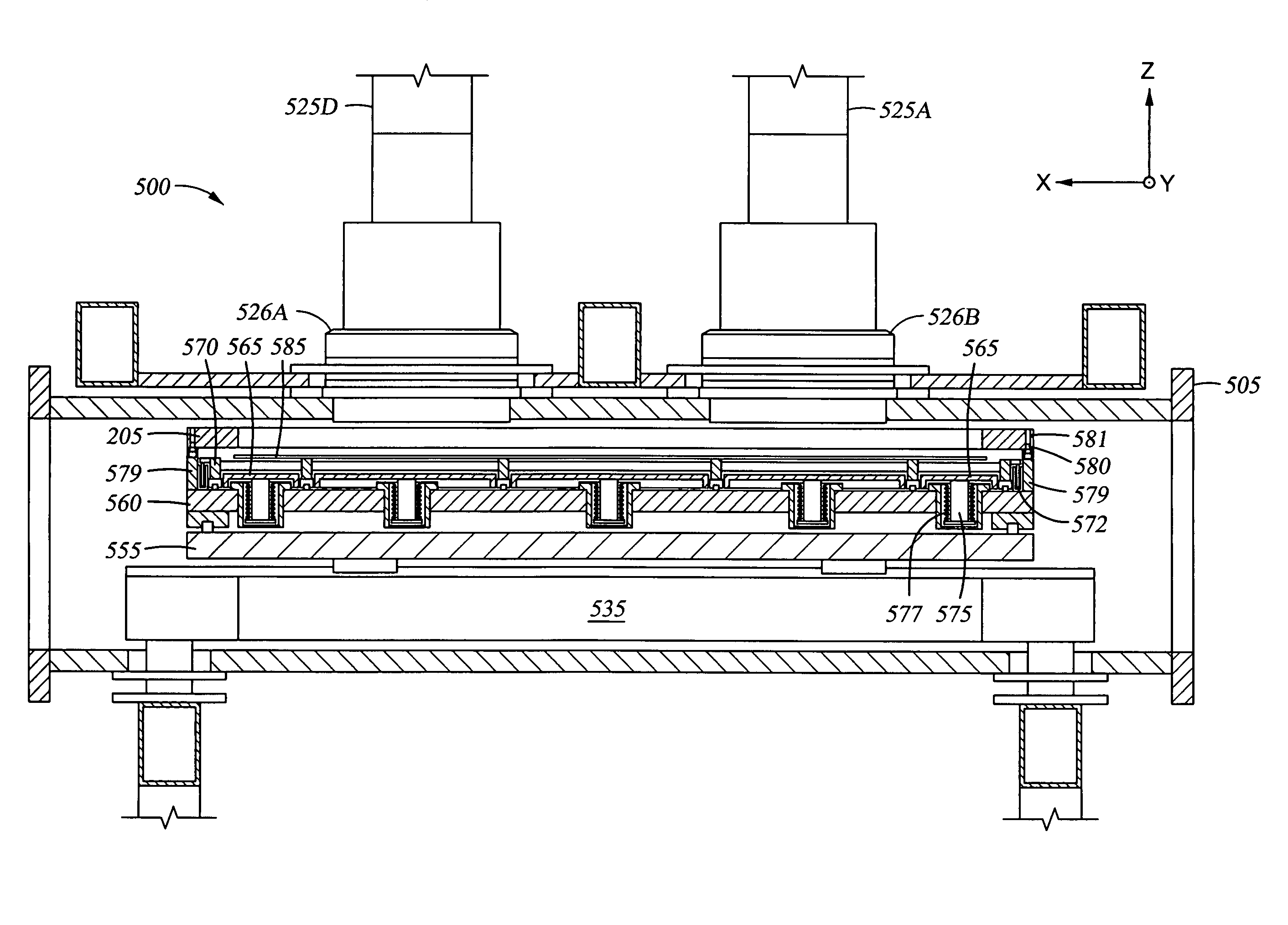
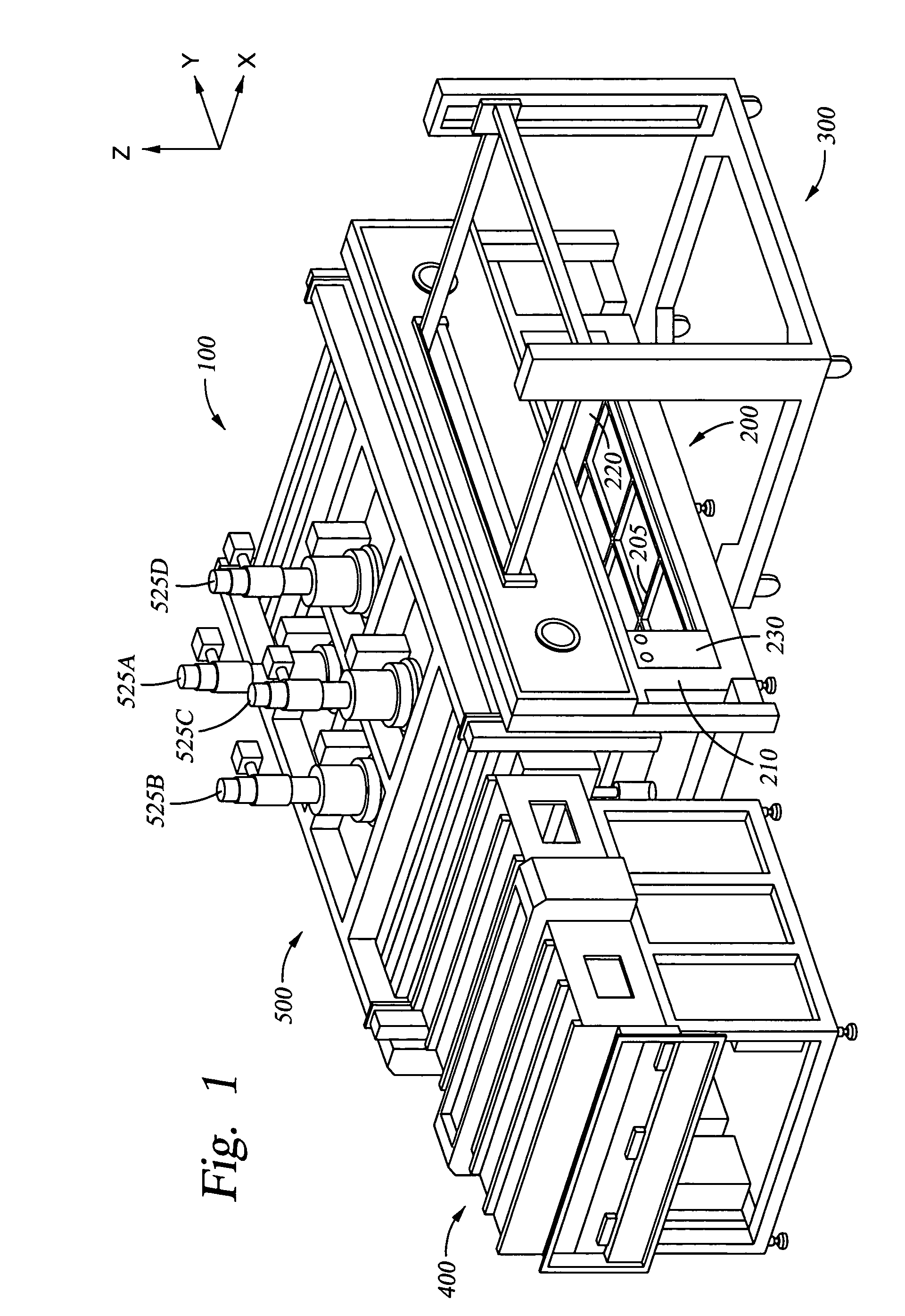
[0027]FIG. 1 shows a schematic view of an electron beam test system 100. The electron beam test system 100 is an integrated system requiring minimum space, and is capable of testing large glass panel substrates, up to and exceeding 1.9 meters by 2.2 meters. As will be described below, the electron beam test system 100 provides stable substrate handling, reduces both substrate and prober alignment time, reduces unwanted particle generation, and provides improved test accuracy, reliability and repeatability.
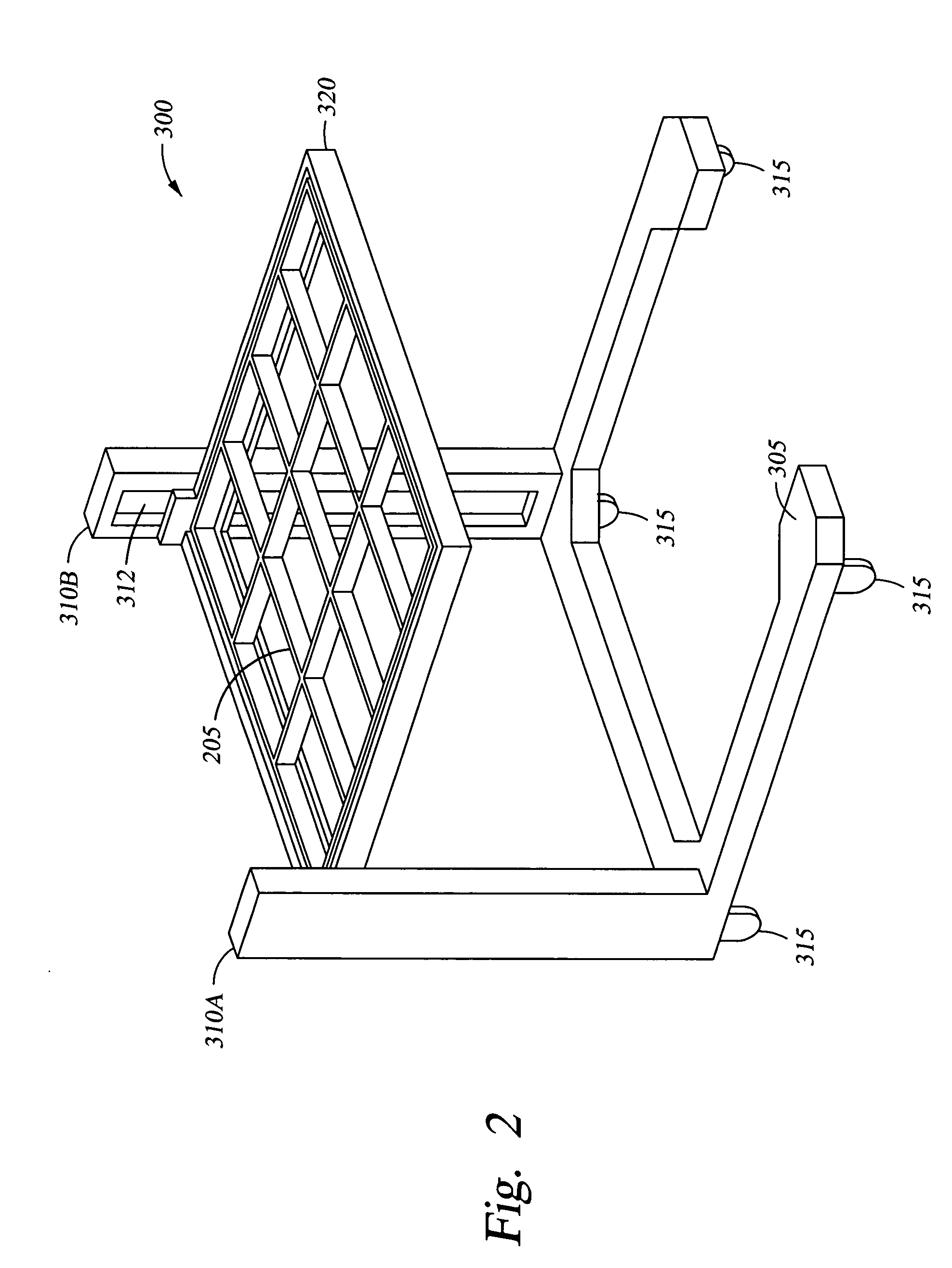
[0028] Referring to FIG. 1, the electron beam test system 100 includes a prober storage assembly 200, a prober transfer assembly 300, a load lock chamber 400, and a testing chamber 500. The prober storage assembly 200 houses one or more probers 205 proximal the test chamber 500 for easy use and retrieval. Preferably, the prober storage assembly 200 is disposed beneath the test chamber 500 as shown in FIG. 1, reducing the clean room space needed for a contaminant free and efficient...
PUM
 Abstract
Description
Claims
Application Information
 - R&D Engineer
- R&D Manager
- IP Professional
- Industry Leading Data Capabilities
- Powerful AI technology
- Patent DNA Extraction
Browse by: Latest US Patents, China's latest patents, Technical Efficacy Thesaurus, Application Domain, Technology Topic, Popular Technical Reports.
© 2024 PatSnap. All rights reserved.Legal|Privacy policy|Modern Slavery Act Transparency Statement|Sitemap|About US| Contact US: help@patsnap.com