Stacked electronic part

Inactive Publication Date: 2005-09-22
KK TOSHIBA
View PDF9 Cites 50 Cited by
  • Summary
  • Abstract
  • Description
  • Claims
  • Application Information

AI Technical Summary

Benefits of technology

[0012] Accordingly, according to an aspect of the present invention, there is provided a stacked electronic part that the generation of bubbles resulting from resin non-filled portions below bonding wires is retarded

Problems solved by technology

In such a structure, however, the semiconductor elements applicable are considerably limited, so that the expansion of the applicability to the semiconductor elements having the same shape and the semiconductor elements that the upper one is larger than the lower one is being conducted.
At that time, if an amount of the resin filled in the space where the bonding wires are arranged is insufficient, there is a problem that a resin non-filled portion is apt to occur below the wires.
As described above, the semiconductor device having a structure that the spacer is arranged between the semiconductor elements has a problem that the resin non-filled portion is apt to occur in the spaces below the bonding wires.
It is also difficult to fill the resin in the resin non-filled portions below the wires in the subsequent resin molding step, so that bubbles resulting from the resin non-filled portions remain.
When bubbles generate in the semiconductor device, separation, leakage or the like is apt to occur resulting from the bubbles in a reliability test on moisture absorption, solder reflow or the like, and the reliability of the semiconductor device is impaired.
But, such a case involves a problem such as oozing out (bleed) of

Method used


Image

  • Stacked electronic part
  • Stacked electronic part
  • Stacked electronic part

Examples


Embodiment Construction

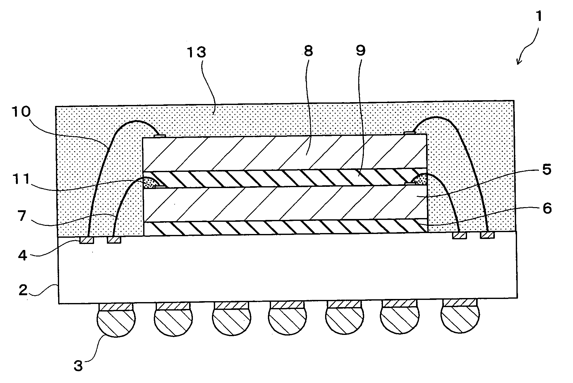
[0033] Modes of conducting the present invention will be described with reference to the drawings. Embodiments of the present invention are described with reference to the drawings, which are provided for illustration only, and the present invention is not limited to the drawings.

[0034]FIG. 1 is a sectional view schematically showing a structure of a first embodiment applying the stacked electronic part of the present invention to a semiconductor device having a stacked multichip configuration. A semiconductor device 1 shown in the drawing has a substrate 2 for mounting elements. The substrate 2 for mounting elements can mount electronic parts, and has a circuit. For the substrate 2, a circuit board in which a circuit is formed to a surface or a inside of an insulating substrate or a semiconductor substrate, or a substrate which integrated a mounting part and a circuit like a leadframe can be applied. The semiconductor device 1 has a circuit board 2 as a substrate for mounting elem...


PUM


Abstract

A stacked electronic part comprises a first electronic part which is adhered onto a circuit board via a first adhesive layer and a second electronic part which is adhered onto the first electronic part via a second adhesive layer. An insulating resin having a filling viscosity of 1 Pa·s or more and less than 1000 Pa·s or a photo-setting insulating resin is filled in the spaces below first bonding wires which are connected to the first electronic part. Thus, the occurrence of bubbles resulting from the resin non-filled portions below the wires can be prevented. Besides, the first electronic part and the second electronic part are adhered via an insulating resin layer having an adhering viscosity of 1 kPa·s or more and 100 kPa·s or less. Therefore, the occurrence of an insulation failure, a short circuit or the like resulting from a contact between the bonding wires of the lower electronic part and the upper electronic part can be prevented.

Description

CROSSREFERENCE TO RELATED APPLICATIONS [0001] This application is based upon and claims the benefit of priority from the prior Japanese Patent Applications No. 2004-078333 and No. 2004-078334, filed on Mar. 18, 2004; the entire contents of which are incorporated herein by reference. BACKGROUND [0002] 1. Field of the Invention [0003] The present invention relates to a stacked electronic part configured by stacking plural electronic parts. [0004] 2. Description of the Related Art [0005] In recent years, to realize miniaturization, high-density packaging and the like of the semiconductor device, there is realized a stacked multichip package which has plural semiconductor elements (semiconductor chips) stacked and sealed in a single package. The stacked multichip package has the plural semiconductor elements sequentially stacked on a circuit board with an adhesive agent such as a die attach material interposed. Electrode pads of each semiconductor element are electrically connected to e...

Claims


Application Information

Patent Timeline
IPC IPC(8): H01L21/58H01L23/02H01L23/28H01L23/31H01L23/48H01L23/52H01L25/065H01L25/07H01L25/10H01L25/18
CPCH01L23/3128H01L2224/451H01L24/48H01L24/83H01L25/0652H01L25/0657H01L2224/05599H01L2224/32145H01L2224/32225H01L2224/45015H01L2224/48091H01L2224/48227H01L2224/484H01L2224/48992H01L2224/49175H01L2224/73215H01L2224/73265H01L2224/83191H01L2224/83855H01L2224/85399H01L2224/8592H01L2225/0651H01L2225/06555H01L2225/06568H01L2225/06575H01L2225/06582H01L2924/01005H01L2924/01006H01L2924/01029H01L2924/01033H01L2924/01078H01L2924/01082H01L2924/014H01L2924/07802H01L2924/09701H01L2924/15311H01L2924/19107H01L2924/20752H01L24/33H01L2924/1815H01L2924/19106H01L25/03H01L2924/0665H01L2924/00014H01L2224/2919H01L24/49H01L2924/00H01L2224/45099H01L2924/00012H01L2924/15787H01L24/45H01L2924/181H01L2224/05554H01L24/73H01L2924/10162
Inventor YOSHIMURA, ATSUSHIOOKUBO, TADANOBUSUGIZAKI, YOSHIAKIHARADA, SUSUMU
Owner KK TOSHIBA
Why Eureka
Try Eureka